ABSTRACT
Nature-inspired architected materials have been widely used to achieve efficient structural materials by harnessing their cellular and hierarchical structures. For example, biological materials observed in bone, shell, nacre, and wood contain constituents, ranging from nanometers to centimeters, arranged in an ordered hierarchy. Because of their composited structures that contain micro and nanoscale building blocks arranged in an ordered hierarchy and the material size effect in the mechanical strength of nano-sized solids, bioceramic materials are mechanically robust and lightweight. The design principles offered by hard biological materials of multiscale composite structures can assist in the creation of advanced ceramic architectures. In addition, the evolution of additive manufacturing technologies has enabled the fabrication of materials with intricate cellular architected materials. In this review, we discussed advanced additive manufacturing for the fabrication of nature-inspired multiscale ceramic structures by combining conformal thin-film coating technique with conventional additive manufacturing methods.
-
KEYWORDS: Ceramic, Additive manufacturing, Multiscale structures, Microlattice, Architected materials, Thin-film coating
-
KEYWORDS: 세라믹, 적층 제조, 멀티스케일 구조, 마이크로 격자 구조, 구조화 재료, 박막 코팅
NOMENCLATURE
Self-Propagating Photopolymer Waveguide
Proximity Field Nanopatterning
Fused Deposition Modeling
Chemical Vapor Deposition
Physical Vapor Deposition
Digital Micromirror Device
Integrated Computational Materials Engineering
1. Introduction
세라믹 재료는 내화학성, 내마모성, 내식성, 내열성 등의 뛰어난 물리적 특성을 장점으로 가지고 있다. 하지만 세라믹 재료는 일반적인 다른 재료에 비해 상대적으로 취성이 강한 특성을 보이기 때문에 복잡한 형상의 가공 및 제조에 어려움이 있고, 이러한 점은 세라믹 재료의 적용 분야를 한정시키는 결정적 요인 중 하나이다. 최근 고분자와 금속 재료용 3D 프린팅 기술의 많은 발전과 더불어, 세라믹 3D 프린팅 기술도 크게 발전하고 있다. 이러한 세라믹 3D 프린팅 기술의 발전을 통해 복잡 형상 제조 및 공정 비용 절감을 이루고 있으며, 기존 금속재료의 대체 뿐만 아니라 획기적인 성능 향상, 새로운 기능 부여 및 추가적인 부가가치를 창출하고 있다. 기존 세라믹 3D 프린팅 기술은 슬러리 기반 방식으로 미세한 세라믹 입자가 골고루 분산되어 있는 세라믹-고분자 혼합재료가 사용된다. 이러한 슬러리 기반 세라믹 3D 프린팅 기술로는 일반적으로 광중합, 잉크젯, 또는 압출 방식을 이용하게 되는데, 통상적으로 전처리된 세라믹-폴리머 복합재료로 3D 프린팅 형상을 제작하고, 적절한 열처리 과정을 통하여 세라믹으로 변환하게 된다. 하지만 기존 세라믹 3D 프린팅 방식에서는 고점도의 세라믹-고분자 혼합체 슬러리로 인하여 고분해능, 멀티스케일, 복잡한 형상의 세라믹 구조체의 제조에 한계가 있었다. 따라서, 본 리뷰에서는 기존 슬러리 방식의 세라믹 3D 프린팅 방식과 다른 박막 코팅(Thin-Film Coating) 방식을 활용하여, 비전통적인 방식으로 제작된 멀티스케일 3D 세라믹 구조의 효율적인 제작기술, 다양한 분야로의 활용 및 한계점에 대해서 소개하고자 한다.
2. Thin Film Deposition Process
2.1 Overview
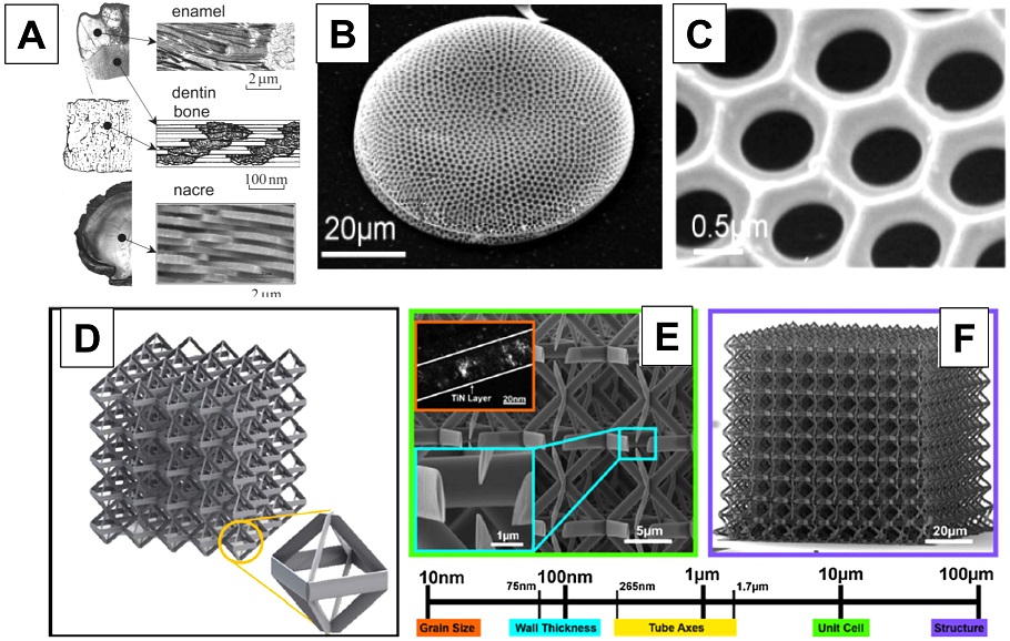
Fig. 1에서 볼 수 있듯이, 자연에서 살펴볼 수 있는 세포 구조와 계층 구조는 기계적으로 효율적인 구조를 얻기 위한 진화의 결과이다. 예를 들어, 뼈, 조개, 진주, 나무에서 관찰되는 딱딱한 생체 물질은 nm에서 cm 스케일까지 계층적 구조로 이루어져 있는 것을 볼 수 있다.
1-3 이러한 생체 세라믹 구조는 물리적으로 견고하고 가벼운데, 이는 마이크로 스케일과 나노 스케일의 빌딩 블록이 규칙적인 계층에 배치된 복합재료 및 나노스케일을 가진 고체의 기계적 강도에서 재료 스케일 효과의 발현에 기인한 것이다.
1-7 멀티스케일 복합 구조의 딱딱한 생체 재료에서 제공하는 설계 원리는 다양한 기능을 보일 수 있는 세라믹 구조를 제작하는 데 도움이 된다. 이 중, 박막을 구조화 재료(Architected Materials)로 변환하는 박막 코팅 기술은 3차원의 구성 요소와 멀티스케일 세라믹 구조 재료(Ceramic Architected Materials)를 제작하기 위해 널리 사용되고 있다.
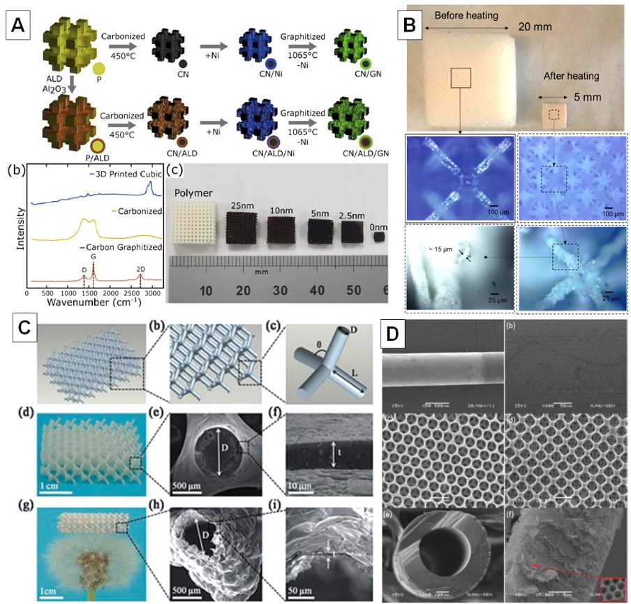
Fig. 1Multiscale composite structures: hard biological materials and artificial architected materials. (a-c) Biological hierarchical lattice materials gain high mechanical robustness from optimized topologies and mechanical size effects in their nanoscale basic building blocks: (a) Vertebral bone and shells,1 (b, c) Whole frustule membrane (External side of the diatom), areola structures (Internal surface of the diatom) in initial stage of formation2 (d-f) Artificial architected materials.8,9 (d) CAD design of a hollow nanolattice, (e) SEM image of the focused ion beam (FIB)-milled edge of a hollow TiN nanolattice, and (f) SEM image of the full structure. The scale at the bottom shows a comparison of the approximate sizes of the components of the structure. (Adapted from Refs. 1, 2, and 9 with permission)

뿐만 아니라, 다양한 박막 재료에 따른 멀티스케일의 복합소재 세라믹 구조도 템플릿에 박막 코팅을 수행하여 제작할 수 있다. 먼저, 템플릿은 Digital Light Processing (DLP), Self-Propagating Photopolymer Waveguide (SPPW), 이광자리소그래피(Two-Photon Lithography, TPL), Proximity Field Nanopatterning (PnP) 등의 광 기반의 적층 제조 방식 중 하나를 통해 제작할 수 있다. 또한, Fused Deposition Modeling (FDM), Direct Ink Writing (DIW), 그리고 Polyjet Printing의 물질 증착 기반의 적층 제조를 이용하여 제조할 수도 있으며, 광범위한 분자 폴리머 또는 입자에서 배합된 인쇄용 잉크의 형태로 수많은 재료를 사용할 수 있지만,
10 고해상도의 복잡한 3D 구조의 프린팅에는 한계가 있다. 한편, 광 기반의 적층 제조는 구조가 매우 복잡하고, 형상 크기가 수십 μm에서 cm의 범위에서 폴리머 형상을 자유롭게 제작할 수 있다.
따라서
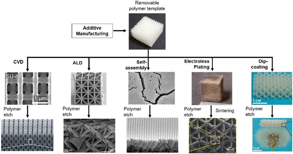
Fig. 2에 보이듯이, 광 기반의 적층 제조와 박막 코팅 공정을 결합하여 멀티스케일 세라믹 구조를 쉽게 제작할 수 있으며, 폴리머 템플릿에 코팅된 박막 재료는 폴리머-세라믹 복합 재료로써 남아있거나, 화학적 또는 열처리를 통해 제거되어 멀티스케일 관형(Tubular) 세라믹 구조체를 형성하는데 이용될 수 있다. 이때, Dip-Coating, Chemical Vapor Deposition (CVD), Physical Vapor Deposition (PVD) 및 Atomic Layer Deposition (ALD)을 포함한 다양한 코팅 방법이 템플릿에 적용될 수 있으며, 이는 수 nm에서 수 μm 범위 두께의 치밀하고 매끄러운 필름 코팅을 가능하게 한다.
4
Fig. 2Converting various thin-film materials into 3D architected materials. Abbreviations: CVD, chemical vapor deposition; ALD, atomic layer deposition4,7,10,11-15 (Adapted from Refs. 7, 11, 13, 14, and 15 with permission)

2.2 Fabrication of Polymeric Template and Post-Processing
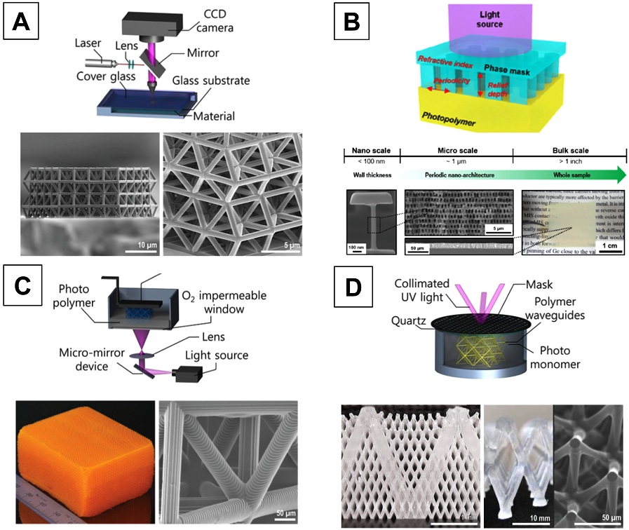
본 절에서는 광 기반의 적층 제조를 이용한 템플릿을 제작하는 방법에 대해서 소개를 하고자 한다.
Fig. 3(a)에서 나타난 TPL은 비선형 광중합 현상을 기반으로 하며, 이를 통해 서브 마이크론 스케일의 높은 분해능을 가지며 복잡한 형상을 구현할 수 있다.
7-12,16-18 이러한 분해능을 바탕으로 TPL은 속이 빈 관형 세라믹 구조 또는 세라믹-고분자 복합체의 고품질 마이크로 구조체의 다양한 물리적 특성을 조사하기 위해 널리 이용되고 있다.
Fig. 3(b)에 보여지듯이, TPL을 통한 3D 나노 프린팅 기술 이외에, PnP는 탄성의 위상 포토마스크와 투명한 레진을 통해 한번의 노광으로 주기적인 복잡한 3D 나노 구조체를 형성할 수 있는 기술이다.
19-22 먼저, 입사하는 빛의 파장에 비슷한 나노 구조물을 가진 탄성 위상마스크를 고체의 광반응성 레진 위에 반데르발스 힘을 통해 물리적으로 접촉시킨다. 완전히 접촉한 후 빛은 마스크를 통과하면서, 광반응성 레진의 내부에 복잡한 3D 광학적 패턴을 형성하게 된다. 이러한 광학적 패턴은 위상마스크, 사용하는 레진의 굴절률, 그리고 빛의 파장 등에 의해 조절이 가능하다. 한 번의 노광 공정으로 나노스케일의 주기적인 3D 형상을 제작할 수 있다는 점은 포토닉스(Photonics),
19 생명 공학, 에너지
21 등의 다양한 분야에서 매력적인 제조기술로 각광을 받고 있다. 하지만, TPL과 PnP의 공간 분해능은 우수한 반면, 처리량(Throughput)이 낮기 때문에 제작 가능한 크기가 크게 제한된다. 한편, 광 기반 적층 제조 기술의 발달로 Digital Micromirror Device (DMD)나 액정 디스플레이를 활용한 DLP 방식이 이러한 처리량의 한계를 극복할 수 있는 대안이 될 수 있다.
Fig. 3Additive manufacturing methods for fabricating polymeric templates. (a) TPL processes focus a laser beam into a photomonomer, creating an ellipsoid-shaped polymer feature (Voxel) down to 100 nm in size,7,9,11 (b) PnP can produce complex and well-defined 3D nanostructures,22 (c) DLP creates centimeter-size arbitrary polymeric microstructures with minimal feature dimensions of 5-300 μm, in a layer-by-layer fashion by polymerizing the surface layer of a photopolymer bath through a digital mask,23 and (d) SPPW creates polymeric microlattices, tens of centimeters in size, within minutes; while topologies are limited to linear extensions of the mask, feature dimensions may be varied in a broad range, from >25 -mm-thick single unit-cell structures to lattices with members ≈10 μm in diameter, to hierarchical structures10,11,26,27 (Adapted from Refs. 10, 11, and 22 with permission)

Fig. 3(c)에 보여지듯이, DLP 방식은 2D 패턴을 한 번의 노광으로 한 레이어를 한번에 경화하고, 이어 수직 방향으로 상하 이동을 통해 3D 형상이 완전히 만들어질 때까지 이를 반복하게 된다.
6,10,23,24 한 레이어에서 광경화되는 두께는 대략 10-100 μm이고, 이는 광경화 레진의 특성, 광원의 출력, 노출 시간, 광개시 제의 농도 등의 복합 효과에 의해서 조절 가능하다. 이러한 DLP 방식은 형상 크기가 수십 μm에서 cm 범위의 복잡한 3D 마이크로 구조의 형성에 적합하다. 단일 층을 지속적으로 쌓아가며 3D 구조를 형성하는 DLP 방식의 적층 제조 방식과는 대조적으로, SPPW 방식은 3D 형상을 부피 단위로 형성할 수 있는 체적 적층 제조 방식(Volumetric Additive Manufacturing)의 하나이다.
Fig. 3(d)에 따르면, SPPW은 광중합 반응을 통해 발생하는 미세한 굴절률의 변화에 의한 광도파로(Optical Waveguide) 효과를 이용하여 빛의 진행 방향으로 광중합 반응이 정렬되는 비선형 광학 현상을 활용한 제조방식이다. SPPW는 최대 두께가 cm 스케일인 단위 셀의 직경이 약 10 μm의 격자 구조체를 빠르게 형성하는데 이용될 수 있다.
4,10,11,25 각각 다른 방향에서 평행하게 조사되는 빛을 주기적인 2D 패턴을 가진 포토마스크에 동시에 노광하면 평행한 빔의 각각의 진행 방향을 따라 고분자섬유다발(Polymeric Fiber Array)이 고분자 레진 안에서 형성된다. 이렇게 형성된 고분자 섬유다발은 서로 교차할 수 있고 이를 통해 주기적인 3D 격자 구조체를 형성하게 된다.
Fig. 4에서 볼 수 있듯이, 광 기반 적층 제조 방법에 의해서 형성된 멀티스케일 3D 폴리머 템플릿은 이후 후처리 공정(Post-Processing)을 통해 세라믹 구조화 재료로 변환될 수 있다. 후처리 공정은 크게 박막 코팅, 폴리머 템플릿 제거, 그리고 변환 과정으로 나눌 수 있다. 대표적인 박막 코팅 방법으로는 CVD, ALD, 자기조립(Self-Assembly), Dip-Coating, 무전해 도금(Electroless Plating)과 같은 방법이 있으며, 폴리머 템플릿의 제거에는 용액에 담가 폴리머를 선택적으로 제거하는 화학적 에칭이나 산소 플라즈마 에칭과 같은 물리적 에칭 방법 등이 주로 사용된다. 이후 변환 과정에서는 Pyrolysis, Calcination, Sintering 등과 같은 열처리 과정을 기반으로 하여 이루어지게 된다. 이렇게 후처리 공정을 거치고 나면 흥미로운 물리적인 특성을 보이는 멀티스케일 세라믹-고분자 복합체 또는 관형 세라믹 구조체가 형성될 수 있다.
Fig. 4Post-processing for synthesizing ceramic-polymer composite or hollow ceramic architectures based on polymer templates. (a) Schematic for fabricating of hollow ceramic and composite architectures by polymer template, thin-film coating, and etching,11 (b) Chemical vapor deposition or atomic layer deposition,25 (c) Self-assembly,30 (d) Dip-coating process28 to better illustrate the dip-coating method, (e) Electroless plating,25 and (f) Heat treatment to remove polymer or material conversion25 (Adapted from Refs. 11, 15, 25, 28 with permission)
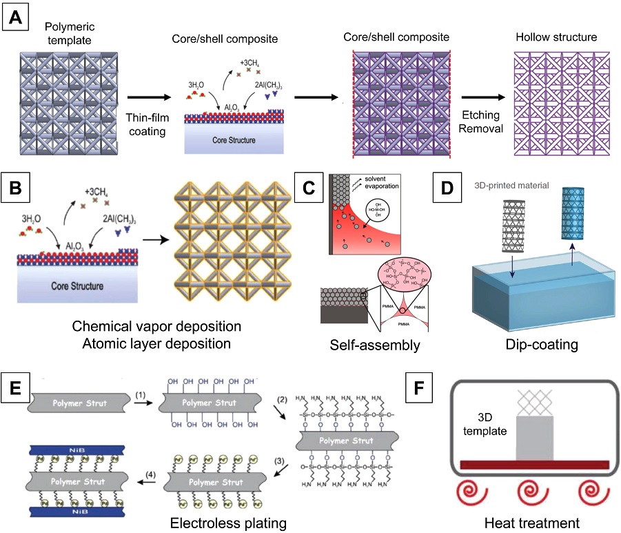
Fig. 4(b)에서 보이듯이, ALD의 경우 복잡한 3D 형상에서 균일하게 나노스케일로 정확하게 코팅 두께 조절이 가능하며 코팅에 있어 방향 의존성이 없기 때문에, 복합구조체를 형성하는데 있어 마이크로-나노스케일 구조화 재료 위에 얇은 세라믹층을 코팅하기 위해 널리 사용되고 있다. 하지만, 매우 느린 코팅 속도는 ALD의 주요 한계점이 지적되고 있다.
Figs. 4(c)와
4(d)에 나와 있듯이, 이와 대조적으로 Dip-Coating이나 자기조립 방식은 재료의 성질이나 종류에 크게 관계없이 간단히 적용할 수 있는 방법으로 알려져 있다. 제작된 폴리머 템플릿을 전구체(Precursor) 용액에 넣고 모든 부분이 균일하게 코팅되도록 할 수 있으며, 이 방법을 통해 폴리머 템플릿을 다양한 코팅 물질과 함께 복합재료 구조체 변환시킬 수 있다.
Fig. 4에 따르면, Dip-Coating 방식의 일종인 무전해 도금 방식 역시 복잡한 형상에 균일하게 박막을 코팅할 수 있도록 잘 확립된 방법이다. 무전해 도금은 화학 반응에 의해 다양한 기판에 금속 또는 합금을 증착하는 과정으로 무전해 도금된 금속 또는 합금 물질은 후속 열처리를 통해 금속 산화물(Metallic Oxides)로 변환할 수 있다. 이러한 무전해 도금 방법은 실제로 얇은 관형 구조물의 제조에 널리 사용되고 있다. 그리고 뒤이어지는 Pyrolysis, Calcination, Sintering과 같은 열처리 공정이 코팅 재료의 세라믹화에 있어 매우 중요하다.
Fig. 4(f)에서 보이듯이, 이러한 열처리는 불활성 분위기, 진공 또는 공기 중 고온에서 유기 물질의 화학적으로 분해하는 과정이며, 가열 중 유기분자는 화학적으로 Glassy 또는 Pyrolytic 탄소로 변화하고 질량이 많이 감소한다. 또한, 고분자 재료의 경우 약 1,000-1,200
oC에서 열처리 과정 중 분해되어 관형 세라믹 구조만 남기고 제거될 수 있다.
2.3 Available Materials with Thin-Film Deposition
3차원 폴리머 템플릿 위에 다양한 박막을 코팅하는 기술은 특정한 기능을 할 수 있도록 표면 특성을 규정하는 중요한 방법이며, 적층 제조에 있어서 가용한 재료의 범위를 확대하는데 중요한 역할을 한다. 특히, 세라믹 박막 증착 기술로서 CVD는 다양한 세라믹 재료를 코팅할 수 있는 유용한 플랫폼을 제공한다.
11,13,14,25,29-32
Fig. 5에서 보여지듯이, 질화규소(SiN), 실리카(SiO
2) 등의 다양한 물질이 코팅된 가벼운 세라믹-폴리머 복합 격자 구조체의 제작에 유용하게 사용될 수 있음을 알 수 있다.
13,29 한편, CVD 방식의 일종인 ALD는 저온 처리가 가능하다는 이점으로 인하여 폴리머 기반의 3D 프린팅 기술에 많이 활용되고 있다. 대표적인 예로, ALD를 통해 얇은 산화알루미늄(Al
2O
3), 질화티타늄(TiN), 실리카 같은 다양한 세라믹 재료를 폴리머 템플릿에 균일하게 코팅하여 멀티스케일 세라믹 마이크로 구조체를 형성하고, 이를 통해 독특한 물리적 특성을 알아보는데 활용할 수 있음이 보고되고 있다.
11,13,14,24,30-32
Fig. 5Multiscale ceramic architectures via CVD and ALD process. (a) Hollow SiO2 lattice manufactured by SPPW, CVD, chemical etching,11,26 (b) Hollow alumina microlattice fabricated by DLP, ALD, and thermal treatment,6 (c) Hollow alumina nanolattice fabricated by TPL, ALD, and O2 plasma etching,11 and (d) Titanium nitride (TiN) nanoshell structure created by PnP, ALD, and microwave plasma etching21 (Adapted from Refs. 6, 11, 21, and 26 with permission)
Figs. 6(a)와
6(b)에 보이는 것처럼 더욱 흥미롭게도, DLP에 의해 제작된 폴리머 격자 구조체에 ALD 방식으로 산화알루미늄 박막을 균일하게 코팅하고, 이어지는 후속 열처리를 통해 발생하는 수축을 제어하여 카본-세라믹 복합재료 및 관형 세라믹 마이크로 격자 구조체의 형성이 보고되고 있다.
32,33 먼저, 세라믹 재료의 코팅을 위한 템플릿 제작을 위해 폴리머를 사용하여 3D 구조물을 제작한다. 그런 다음, 기능성 세라믹 재료를 폴리머 지지체 위에 코팅한 후, 통상적인 열처리 과정과 비교하여 빠른 온도 증가 속도의 열처리 과정을 통해 폴리머 물질을 제거함과 동시에 제어된 방식으로 수축시킨다. 이를 통해 수 μm에서 수십 μm 사이즈를 지닌 멀티스케일 세라믹 관형 격자 구조를 형성할 수 있게 된다. 이러한 제작 기술은 열처리 전 코팅된 세라믹 박막의 두께에 따라 격자 구조의 수축 비율과 표면 주름의 정도를 제어할 수 있다.
32 이러한 제작 방법은 실질적으로 다양한 물리적 특성을 가지는 세라믹 구조체 형성으로 확장될 수 있을 것으로 예상될 뿐만 아니라, 세라믹 구조의 주름진 표면은 넓은 표면적을 지닌 촉매 지지체로서의 활용을 기대할 수 있게 한다. 다음으로
Figs. 6(c)와
6(d)와 같이 저렴한 비용으로 이미 잘 발전된 코팅 기술로써 Dip-Coating
14과 자기조립
15,34-38을 활용하여 폴리머 템플릿에 박막 코팅을 수행할 수 있다. 예를 들어, 3D 폴리머 구조의 표면에 Dip-Coating 및 후속 열처리 과정을 통해 실리카-고분자 복합체 및 관형 실리카 격자 구조를 형성할 수 있고, 이러한 구조화 재료는 기계적 강도 및 열적 안정성을 향상할 수 있는 것으로 나타났다. 또한 자기조립 방법은 저렴한 비용으로 나노 스케일의 다공성 세라믹 구조체를 얻을 수 있다는 점에서 상당한 관심을 모으고 있다. 예를 들어, 콜로이드 결정(Colloidal Crystal)은 100-300 nm 지름의 콜로이드 입자를 물 또는 알코올에 분산시킨 후 용매를 서서히 증발시키면서, 이때 발생하는 모세관 힘에 의해 면심입방(Face Centered Cubic, FCC)의 주기적인 결정 구조를 얻을 수 있다. 콜로이드 결정은 보석의 일종인 오팔(Opal)과 구조 및 생성 원리가 동일하므로 인공 오팔로 불리는데, 이러한 콜로이드 입자의 자기조립을 활용하면 나노스케일의 매우 균일하고 주기적인 역오팔(Inverse Opal) 구조를 생성 할 수 있다.
15,34-38 Fig. 6(d)에 보이듯이,
35 이러한 역오팔 구조는 매우 균일한 크기와 주기적인 기공 분포를 갖춘 연결된 다공성 구조체의 특성을 보인다. 자기조립을 통해 상호 연결된 세라믹 박막이 저렴한 비용으로 대면적 형성이 가능하며, 이는 광결정, 세포 배양 지지체, 센서, 또는 촉매 지지체 등으로 다양하게 활용될 수 있다.
Fig. 6Ceramic architectures via volumetric shrinkage and, self-assembly, and dip-coating. (a) Graphene/ceramic/carbon composited architecture via the isotropic shrinkage and conversion of a polymeric lattice to graphene network.32 Optical images demonstrating an 80% shrinkage in each direction occurs after process completion resulting in an over 125× reduction in volume, (b) Hollow alumina microarchitectures fabricated by DLP, ALD, and volumetric shrinkage controlled via calcination in the air,33 (c) The architecture of the SiO2/polymer and hollow SiO2 lattices formed by DLP, dip-coating, and calcination,14 and (d) Silica inverse opal film by self-assembly and heat treatment35 (Adapted from Refs. 14, 32, 33, and 35 with permission)
2.4 Various Physical Properties
복잡한 형상의 폴리머 템플릿에 다양한 박막 세라믹 재료를 코팅함으로써 멀티스케일 세라믹 구조체를 제조할 수 있으며, 특히 이 방법은 관형 마이크로 구조물의 손쉬운 제작을 가능하게 한다. 이렇게 비전통 방식으로 제작된 멀티스케일 세라믹 구조체는 가벼우면서 기계적 특성이 뛰어난 기계적 메타 물질, 효율적인 열 및 전기 절연체 구조, 광결정 구조, 촉매 지지체와 같은 다양한 응용 분야에 활용될 수 있도록 토폴로지를 포함한 3D 형상의 조합 및 재료 특성에 따라 설계될 수 있다. 먼저, 멀티스케일의 구조화 재료의 개념은 매우 가볍고, 강하고 질긴 세라믹 메타 물질을 구현할 수 있게 한다.
4-7,12,18
DLP 및 TPL 등의 광 기반 적층 제조 기술을 이용하면 다양한 형상의 Stretching-Dominant 격자 구조를 형성할 수 있고,
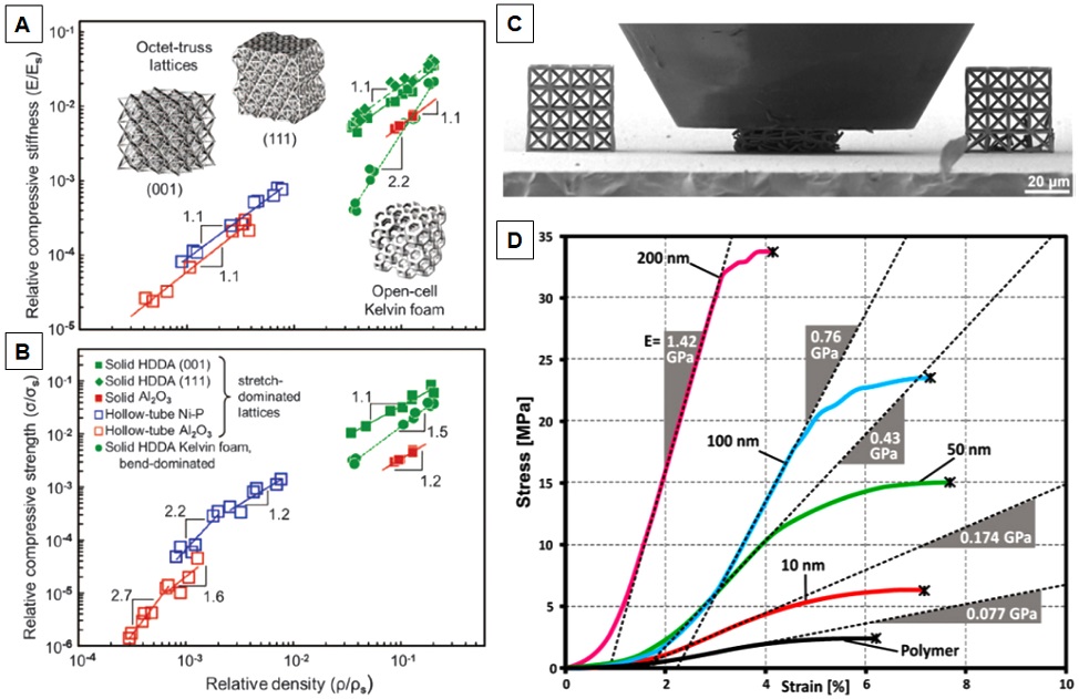
Figs. 7(a)와
7(b)에서 보이듯이, 압축력이 가해지는 상황에서 관형 세라믹 격자 구조의 상대 밀도(
ρ)에 대한 강성(
E) 및 강도(
σ)의 거동이 이론적인 예측(
E ∝
ρ and
σ ∝
ρ)과 거의 일치함을 확인할 수 있다.
6 또한
Figs. 7(c)와
7(d)에서 알 수 있듯이, TPL과 ALD를 사용하여 제작된 나노스케일의 세라믹-폴리머 격자 구조의 경우, 1,000 kg/m
3의 아주 낮은 밀도에서 최대 280 MPa의 압축 강도를 가지는 것을 확인함으로써, 멀티스케일 세라믹 복합구조체의 우수한 기계적 특성을 나타내는 결과가 보고되고 있다.
7
Fig. 7Lightweight structures and metamaterials. (a) Relative stiffness and (b) relative strength as a function of relative density for hollow ceramic microlattices.6 (c) An in situ test of a polymer/ceramic composite nanolattices, and (d) Stress-strain curves of nanolattices.7 Alumina layers of the indicated thicknesses have been deposited onto a 3D polymeric template. With increasing layer thickness, the compressive strength and stiffness increase strongly compared with bare polymeric templates (Adapted from Refs. 6 and 7 with permission)
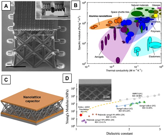
한편, 3D 형상과 세라믹 구조화 재료에 따라 구조의 열적, 전기적 특성 제어도 가능하다.
Figs. 8(a)와
8(b)에 따르면, 최근 관형 세라믹(Al
2O
3) 격자 구조의 경우 우수한 기계적 성능과 함께 뛰어난 단열 특성을 가질 수 있음이 보고되었다.
16 격자 구조의 형상, 단위 셀 크기, 스케일 등의 기하학적인 요인들이 세라믹 격자 구조체의 열전달 특성에 큰 영향을 미치는데, 측정된 관형 세라믹 나노 격자의 열전도율은 2 mW m
-1K
-1로써, 추후 마이크로 스케일의 디바이스에서 효율적인 단열 구조로써 역할을 수행할 수 있을 것으로 기대한다.
Fig. 8(b)는 멀티스케일 세라믹 구조화 재료의 다기능 성능을 보여주고 있는데, 이는 관형 세라믹 나노 격자 구조가 매우 낮은 열전도율과 높은 강성 및 강도를 동시에 보일 수 있다는 것을 의미한다. 이와 더불어
Figs. 8(c)와
8(d)에 보이듯이, 관형 세라믹 나노 격자 구조는 매우 낮은 유전율(k)을 가질 수 있는데, 이러한 Low-k 세라믹 나노 구조화 재료는 매우 주기적인 다공성 구조로 인해 마이크로 전자 및 장치의 기계적 탄성 및 열 안정성을 갖춘 커패시터로 활용을 기대할 수 있다.
17
Fig. 8Multifunctional performance of hollow ceramic nanoarchitected materials. (a) SEM image of hollow alumina nanolattice,39 (b) Material property plot of specific modulus versus thermal conductivity. For the same specific stiffness, hollow alumina nanolattices achieve an order of magnitude lower thermal conductivity than do polymer foams and porous ceramics used for space shuttle thermal protection systems, (c) Schematics of hollow ceramic nanolattice capacitor,17 and (d) Young’s modulus vs dielectric constant plots of the nanolattice compared with other Low-k materials (Adapted from Refs. 17 and 39 with permission)

광결정(Photonic Crystal)은 물질의 광학적인 성질을 이용할 수 있는 구조로 되어 있거나 구조를 갖도록 인공적으로 만들어 낸 물질을 의미하는 것으로 빛의 파장과 비슷한 길이의 격자 주기 구조를 갖는 물질이다.
이러한 광결정의 고유한 특성은 특정 영역에서 빛이 통과할 수 없는 대역을 의미하는 Photon Band Gap (PBG)에서 비롯된다고 할 수 있다. 광결정 구조는 1, 2, 3차원 구조로 생각해볼 수 있고, 이 구조들은 모두 PBG를 조절함으로써 빛을 공동(Cavity)에 가두거나 도파관(Waveguide)에 가둘 수 있도록 조작가능한 기반을 마련할 수 있다.
따라서, 제어 가능한 PBG를 갖춘 광결정은 효율적인 마이크로 웨이브 안테나, 마이크로 레이저, 광섬유 센서, 또는 디스플레이 장치를 포함하는 새로운 분야로의 활발한 응용이 기대된다. 이러한 측면에서, 앞 절에서 설명한 Dip-Coating, 자기조립 방법은 효율적으로 나노스케일의 3D 광결정 구조를 제작하는데 활용할 수 있다. 예를 들어
Figs. 9(a)와
9(b)에서 알 수 있듯이, 다양한 용매에서 광학 특성이 변화하는 센서를 개발하기 위해 역오팔 실리카 광결정 구조를 Dip-Coating과 자기조립 방법을 활용하여 제작할 수 있다.
37,38 폴리머 콜로이드 입자를 실리카 기반의 전구체 용액에 혼합하고, 자기조립을 통해 주기적인 폴리머 콜로이드 입자의 결정구조를 얻는다.
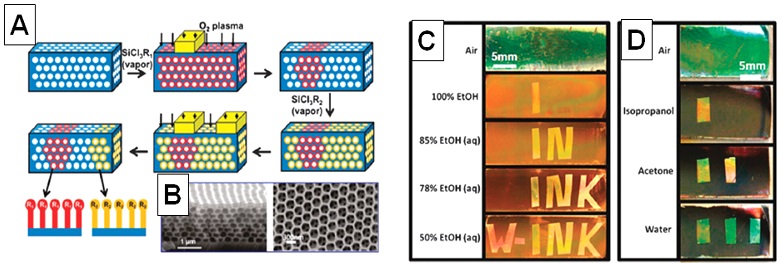
Fig. 9Ceramic architected materials with photonic and optical applications. (a) Schematic of the chemical encoding procedure of the inner surfaces of the inverse opal films, (b) SEM image of the inverse opal films,37 (c) Optical images of an inverse opal film in which the word ‘‘W-INK’’ is encoded via the surface chemistry in the film, and (d) Optical images of a film encoded with three bars displaying distinct optical patterns when immersed in the common solvents, water, acetone, and isopropanol (Adapted from Ref. 37 with permission)

Fig. 9(b)에서 볼 수 있듯이, 후속 열처리를 통해 폴리머 콜로이드 입자를 제거함과 동시에, 실리카 기반의 매우 균일한 다공성 역오팔 구조를 얻을 수 있다. 이후 각각의 포토마스크를 이용한 스텐실 플라즈마 처리를 수행하여 각 영역에서 다른 젖음 특성을 보이는 패턴을 가질 수 있도록 실리카 역오팔 구조의 표면 특성을 개질할 수 있다.
Figs. 9(c)와
9(d)에서 보이듯이, 이후 실리카 역오팔 구조를 특정 액체에 담그면 국소적인 침투가 발생하여 특정 광학 패턴을 형성하게 되는데, 이러한 플랫폼은 향후 위조 방지 또는 비색(Colorimetric) 지표로서의 활용이 기대된다.
또한 나노 및 마이크로 스케일 구조는 가벼우며, 넓은 표면적의 다공성 구조, 그리고 균일한 유동 분포를 담보하는 3D 구조에 의해 촉매 반응의 효율을 높일 수 있다.
10 예를 들어
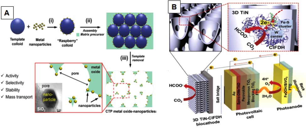
Fig. 10(a)에서 보이듯이, Dip-Coating과 자기조립 방식을 통해 촉매 금속이 포함된 금속-세라믹 다공성 구조체를 매우 균일하게 형성할 수 있으며,
40,41 Fig. 10(b)에서 알 수 있듯이, 이를 통해 메탄올과 에탄올을 모두 선택적으로 산화하여 높은 변환 효율로 변환하는 효율적인 촉매 지지체로서의 성능을 검증할 수 있었다. 마찬가지로 PnP 및 ALD 공정에 의해 형성된 3D 다공성 세라믹 구조체의 효율적 촉매 반응에 기반한 효과적인 탄소 저감 기술의 가능성을 살펴볼 수 있다.
21 이러한 높은 효율의 촉매 반응은 멀티스케일 3D 세라믹 구조의 도입에 의한 빠른 열 응답 및 균일한 유동 흐름 분포에 의한 것으로 판단할 수 있다.
Fig. 10Electrochemical devices and catalytic supports. (a) Schematic of the synthesis of metal nanoparticles embedded in silica porous materials.40 Inset in the bottom shows a TEM image of a nanoparticle partially entrenched into the silica matrix, and (b) Schematic illustration of 3D-structured, electrically conductive TiN nanoshells for biocatalytic CO2-to-formate conversion21 (Adapted from Refs. 21 and 40 with permission)
3. Challenges
일반적으로 적층 제조 공정과 박막 코팅 공정을 통한 멀티스케일 세라믹 구조화 재료는 재료 자체의 고유 결함과 제조 공정에서 발생하는 결함에 의해서 많은 영향을 받는다. 또한 재료 내에서 복잡한 응력 상태, 불규칙한 균열, 제조에 기인하는 기하학적 결함의 존재에 의해 멀티스케일 세라믹 구조체의 기계적 특성(강성, 강도 등)의 정확한 예측이 어렵다.
42-44 이러한 결함들로 인하여 관형 세라믹 구조화 재료의 경우 실험적으로 측정된 강성과 강도는 이론적 접근과 수치 모델에 의해 예측된 것보다 항상 크게 낮은 것으로 나타나고 있다.
42,43 이러한 차이는 간단한 모델에서 예측하기 힘든 복잡한 응력 상태와 제조 공정에서 기인한 기하학적 결함의 존재로 인한 것이라고 판단된다.
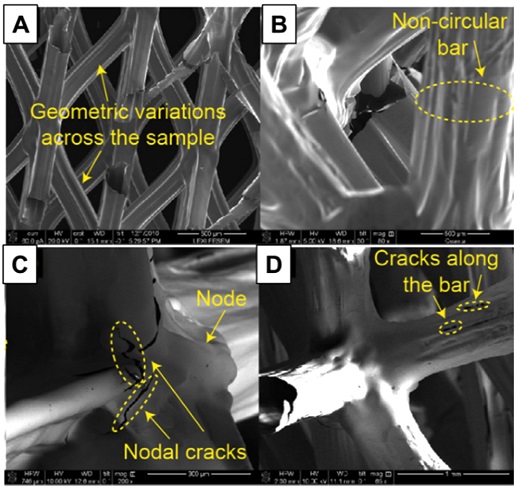
Fig. 11은 관형 격자 구조의 결함의 원인을 파악하기 위한 SEM 측정 결과를 보여주고 있는데, 기하학적 특성의 변화, 절점에서의 기하학적 결함, 절점에서의 균열 등의 결함이 일반적으로 관찰됨을 확인할 수 있다.
Fig. 11 Typical geometric defects observed in architected materials with thin-film deposition process. (a-b) Geometric properties variations, and (c-d) Geometric imperfections at nodes and nodal cracks42 (Adapted from Ref. 42 with permission)

한편, 멀티스케일 세라믹 구조화 재료의 다양한 기능을 예측하고 최적화하기 위해서 멀티스케일 모델링이 필요하다.
44 하지만 기존의 많은 시도에도 불구하고, 설계된 재료의 복잡한 비선형/비탄성 동적 응답 특성과 재료와 구조의 스케일이 유사한 멀티스케일 구조의 특성으로 인하여 많은 어려움이 있다. 이러한 문제를 해결하기 위해 최근 수치적 해석 방법과 재료의 미세 구조 및 나노 스케일의 메커니즘을 정확하게 설명할 수 있는 원자론적 방법을 결합한 종합전산재료공학(Integrated Computational Materials Engineering, ICME)을 활용한 방법이 주목을 받고 있다. 연속체 수준의 모델링 및 토폴로지 최적화와 결합하여 재료와 구조의 공동 설계를 가능하게 할 것으로 생각되며, 실험적으로 얻어진 실질적인 3차원적인 자료를 기계적 성질 예측을 위한 모사 연구에 활용함으로써 멀티스케일 세라믹 구조화 재료의 모델링과 최적화 방안을 제시할 수 있을 것으로 기대한다.
4. Conclusions
본 리뷰에서는 기존의 슬러리 방식의 세라믹 3D 프린팅 방식으로 구현하기 어려운 멀티스케일 세라믹 구조화 재료의 제작 방법, 이에 대한 활용 및 한계점에 대해서 살펴보았다. 최근 많은 관심을 받고 있으며 다양한 분야로의 활발한 융합이 일어나고 있는 기술이 적층 제조 기술이지만, 세라믹 적층 제조 기술은 다른 재료 대비 기술 발전이 더디어 왔던 것은 사실이다. 하지만 적층 제조 기술은 세라믹 재료의 난성형성을 해결하며 세라믹 재료의 적용 범위 확대에 큰 기회를 제공하였으며, 난성형성의 기술적 한계를 계속 극복해 나간다면, 새로운 부가적인 가치 창출이 예상되는 기회의 기술이기도 하다.
한편, 멀티스케일 세라믹 구조화 재료는 우수한 기계적 특성 및 다양한 분야로의 폭넓은 활용 가치를 지니고 있다. 예를 들어, 바이오 세라믹 스캐폴드의 경우 복잡한 다공성 3D 구조 및 다양한 종류의 소재 활용 가능성이 더 중요한 요소이므로 앞서 살펴 본 멀티스케일 세라믹 구조체 제작 방법이 적합하다고 볼 수 있다. 하지만, 현재 본 리뷰에서 소개한 기술개발 단계는 아직 개념과 가능성만이 제시된 단계이며 광범위하게 사용하기에는 아직 많은 제약이 존재한다. 따라서, 적층 제조 공정 및 박막 코팅 공정의 다양한 소재 개발, 제조 공정 최적화, 그리고 ICME를 활용한 멀티스케일 모델링을 통해 멀티스케일 세라믹 구조체의 적용 범위를 넓히고 실험실 수준을 벗어나 광범위하게 활용되기를 기대한다.
ACKNOWLEDGMENTS
이 논문은 2021-2022년도 창원대학교 자율연구과제 연구비 지원으로 수행된 연구결과임.
REFERENCES
- 1.
Gao, H., Ji, B., Jäger, I. L., Arzt, E., and Fratzl, P., “Materials Become Insensitive to Flaws at Nanoscale: Lessons from Nature,” Proceedings of the National Academy of Sciences, Vol. 100, No. 10, pp. 5597-5600, 2003.
10.1073/pnas.0631609100
- 2.
Losic, D., Mitchell, J. G., Lal, R., and Voelcker, N. H., “Rapid Fabrication of Micro- and Nanoscale Patterns by Replica Molding from Diatom Biosilica,” Advanced Functional Materials, Vol. 17, No. 14, pp. 2439-2446, 2007.
10.1002/adfm.200600872
- 3.
Jang, D., Meza, L. R., Greer, F., and Greer, J. R., “Fabrication and Deformation of Three-Dimensional Hollow Ceramic Nanostructures,” Nature Materials, Vol. 12, No. 10, pp. 893-898, 2013.
10.1038/nmat3738
- 4.
Schaedler, T. A. and Carter, W. B., “Architected Cellular Materials,” Annual Review of Materials Research, Vol. 46, pp. 187-210, 2016.
10.1146/annurev-matsci-070115-031624
- 5.
Martin, J. H., Ashby, D. S., and Schaedler, T. A., “Thin-Walled High Temperature Alloy Structures Fabricated from Additively Manufactured Polymer Templates,” Materials & Design, Vol. 120, pp. 291-297, 2017.
10.1016/j.matdes.2017.02.023
- 6.
Zheng, X., Lee, H., Weisgraber, T. H., Shusteff, M., DeOtte, J., et al., “Ultralight, Ultrastiff Mechanical Metamaterials,” Science, Vol. 344, No. 6190, pp. 1373-1377, 2014.
10.1126/science.1252291
- 7.
Bauer, J., Hengsbach, S., Tesari, I., Schwaiger, R., and Kraft, O., “High-Strength Cellular Ceramic Composites with 3D Microarchitecture,” Proceedings of the National Academy of Sciences, Vol. 111, No. 7, pp. 2453-2458, 2014.
10.1073/pnas.1315147111
- 8.
Meza, L. R. and Greer, J. R., “Mechanical Characterization of Hollow Ceramic Nanolattices,” Journal of Materials Science, Vol. 49, No. 6, pp. 2496-2508, 2014.
10.1007/s10853-013-7945-x
- 9.
Chen, Z., Li, Z., Li, J., Liu, C., Lao, C., et al., “3D Printing of Ceramics: A Review,” Journal of the European Ceramic Society, Vol. 39, No. 4, pp. 661-687, 2019.
10.1016/j.jeurceramsoc.2018.11.013
- 10.
Kim, S., Kim, D. H., Kim, W., Cho, Y. T., and Fang, N. X., “Additive Manufacturing of Functional Microarchitected Reactors for Energy, Environmental, and Biological Applications,” International Journal of Precision Engineering and Manufacturing-Green Technology, Vol. 8, No. 1, pp. 303-326, 2021.
10.1007/s40684-020-00277-5
- 11.
Bauer, J., Meza, L. R., Schaedler, T. A., Schwaiger, R., Zheng, X., et al., “Nanolattices: An Emerging Class of Mechanical Metamaterials,” Advanced Materials, Vol. 29, No. 40, Paper No. 1701850, 2017.
10.1002/adma.201701850
- 12.
Meza, L. R., Das, S., and Greer, J. R., “Strong, Lightweight, and Recoverable Three-Dimensional Ceramic Nanolattices,” Science, Vol. 345, No. 6202, pp. 1322-1326, 2014.
10.1126/science.1255908
- 13.
Tétreault, N., von Freymann, G., Deubel, M., Hermatschweiler, M., Pérez-Willard, F., et al., “New Route to Three-Dimensional Photonic Bandgap Materials: Silicon Double Inversion of Polymer Templates,” Advanced Materials, Vol. 18, No. 4, pp. 457-460, 2006.
10.1002/adma.200501674
- 14.
Wei, F., Zhou, Y., Yang, Q., Guo, L., and Jiang, L., “Silica Film Deposited on Diamond-Structured Polymer Microlattices by Dip Coating,” RSC Advances, Vol. 7, No. 86, pp. 54668-54673, 2017.
10.1039/C7RA09297K
- 15.
Hatton, B., Mishchenko, L., Davis, S., Sandhage, K. H., and Aizenberg, J., “Assembly of Large-Area, Highly Ordered, Crack-Free Inverse Opal Films,” Proceedings of the National Academy of Sciences, Vol. 107, No. 23, pp. 10354-10359, 2010.
10.1073/pnas.1000954107
- 16.
Portela, C. M., Vidyasagar, A., Krödel, S., Weissenbach, T., Yee, D. W., et al., “Extreme Mechanical Resilience of Self-Assembled Nanolabyrinthine Materials,” Proceedings of the National Academy of Sciences, Vol. 117, No. 11, pp. 5686-5693, 2020.
10.1073/pnas.1916817117
- 17.
Lifson, M. L., Kim, M. W., Greer, J. R., and Kim, B. J., “Enabling Simultaneous Extreme Ultra Low-k in Stiff, Resilient, and Thermally Stable Nano-Architected Materials,” Nano Letters, Vol. 17, No. 12, pp. 7737-7743, 2017.
10.1021/acs.nanolett.7b03941
- 18.
Jang, D., Meza, L. R., Greer, F., and Greer, J. R., “Fabrication and Deformation of Three-Dimensional Hollow Ceramic Nanostructures,” Nature Materials, Vol. 12, No. 10, pp. 893-898, 2013.
10.1038/nmat3738
- 19.
Jeon, S., Nam, Y. S., Shir, D. J. L., Rogers, J. A., and Hamza, A., “Three Dimensional Nanoporous Density Graded Materials Formed by Optical Exposures through Conformable Phase Masks,” Applied Physics Letters, Vol. 89, No. 25, Paper No. 253101, 2006.
10.1063/1.2405386
- 20.
Na, Y. E., Shin, D., Kim, K., Ahn, C., Jeon, S., et al., “Emergence of New Density-Strength Scaling Law in 3D Hollow Ceramic Nanoarchitectures,” Small, Vol. 14, No. 44, Paper No. 1802239, 2018.
10.1002/smll.201802239
- 21.
Kuk, S. K., Ham, Y., Gopinath, K., Boonmongkolras, P., Lee, Y., et al., “Continuous 3D Titanium Nitride Nanoshell Structure for Solar-Driven Unbiased Biocatalytic CO2 Reduction,” Advanced Energy Materials, Vol. 9, No. 25, Paper No. 1900029, 2019.
10.1002/aenm.201900029
- 22.
Bae, G., Jang, D., and Jeon, S., “Scalable Fabrication of High-Performance Thin-Shell Oxide Nanoarchitected Materials via Proximity-Field Nanopatterning,” ACS Nano, Vol. 15, No. 3, pp. 3960-3970, 2021.
10.1021/acsnano.0c10534
- 23.
Zheng, X., Smith, W., Jackson, J., Moran, B., Cui, H., et al., “Multiscale Metallic Metamaterials,” Nature Materials, Vol. 15, No. 10, pp. 1100-1106, 2016.
10.1038/nmat4694
- 24.
Zhao, Y., Wei, F., Zhao, X., Yang, Q., Guo, L., et al., “Effect of Phosphorus Content on Mechanical Properties of Polymeric Nickel Composite Materials with a Diamond-Structure Microlattice,” RSC Advances, Vol. 8, No. 58, pp. 33025-33029, 2018.
10.1039/C8RA04695F
- 25.
Zhang, X., Wang, Y., Ding, B., and Li, X., “Design, Fabrication, and Mechanics of 3D Micro-/Nanolattices,” Small, Vol. 16, No. 15, Paper No. 1902842, 2020.
10.1002/smll.201902842
- 26.
Maloney, K. J., Roper, C. S., Jacobsen, A. J., Carter, W. B., Valdevit, L., et al., “Microlattices as Architected Thin Films: Analysis of Mechanical Properties and High Strain Elastic Recovery,” APL Materials, Vol. 1, No. 2, Paper No. 022106, 2013.
10.1063/1.4818168
- 27.
Schaedler, T. A., Jacobsen, A. J., Torrents, A., Sorensen, A. E., Lian, J., et al., “Ultralight Metallic Microlattices,” Science, Vol. 334, No. 6058, pp. 962-965, 2011.
10.1126/science.1211649
- 28.
Ragelle, H., Tibbitt, M. W., Wu, S. Y., Castillo, M. A., Cheng, G. Z., et al., “Surface Tension-Assisted Additive Manufacturing,” Nature Communications, Vol. 9, No. 1, pp. 1-10, 2018.
10.1038/s41467-018-03391-w
- 29.
Zhou, Y. F., Yao, C. Z., Yang, Q. L., Guo, L., and Jiang, L., “Mechanical Properties of Diamond-Structured Polymer Microlattices Coated with the Silicon Nitride Film,” Advanced Engineering Materials, Vol. 18, No. 2, pp. 236-240, 2016.
10.1002/adem.201500424
- 30.
Ozaydin-Ince, G., Coclite, A. M., and Gleason, K. K., “CVD of Polymeric Thin Films: Applications in Sensors, Biotechnology, Microelectronics/Organic Electronics, Microfluidics, MEMS, Composites and Membranes,” Reports on Progress in Physics, Vol. 75, No. 1, Paper No. 016501, 2011.
10.1088/0034-4885/75/1/016501
- 31.
Ahn, J., Ahn, C., Jeon, S., and Park, J., “Atomic Layer Deposition of Inorganic Thin Films on 3D Polymer Nanonetworks,” Applied Sciences, Vol. 9, No. 10, Paper No. 1990, 2019.
10.3390/app9101990
- 32.
Nakanishi, K. and Hofmann, S., “Ordered Graphitic Microfoams via Shrinkage and Catalytic Conversion of Polymer Scaffolds,” APL Materials, Vol. 8, No. 2, Paper No. 021106, 2020.
10.1063/1.5136235
- 33.
Kim, S., “3D printing of Hollow Biocompatible Ceramic Scaffold by Material Deposition and Volumetric Shrinkage,” Journal of the Korean Society of Manufacturing Technology Engineers, Vol. 28, No. 1, pp. 31-36, 2019.
10.7735/ksmte.2019.28.1.31
- 34.
Phillips, K. R., Shirman, T., Shirman, E., Shneidman, A. V., Kay, T. M., et al., “Nanocrystalline Precursors for the Co-Assembly of Crack-Free Metal Oxide Inverse Opals,” Advanced Materials, Vol. 30, No. 19, Paper No. 1706329, 2018.
10.1002/adma.201706329
- 35.
Haibin, N., Ming, W., and Wei, C., “Sol-Gel Co-Assembly of Hollow Cylindrical Inverse Opals and Inverse Opal Columns,” Optics Express, Vol. 19, No. 27, pp. 25900-25910, 2011.
10.1364/OE.19.025900
- 36.
Zhou, N., Zhang, A., Shi, L., and Zhang, K. Q., “Fabrication of Structurally-Colored Fibers with Axial Core-Shell Structure via Electrophoretic Deposition and Their Optical Properties,” ACS Macro Letters, Vol. 2, No. 2, pp. 116-120, 2013.
10.1021/mz300517n
- 37.
Burgess, I. B., Mishchenko, L., Hatton, B. D., Kolle, M., Loncar, M., et al., “Encoding Complex Wettability Patterns in Chemically Functionalized 3D Photonic Crystals,” Journal of the American Chemical Society, Vol. 133, No. 32, pp. 12430-12432, 2011.
10.1021/ja2053013
- 38.
Vasquez, Y., Kolle, M., Mishchenko, L., Hatton, B. D., and Aizenberg, J., “Three-Phase Co-Assembly: In Situ Incorporation of Nanoparticles into Tunable, Highly Ordered, Porous Silica Films,” ACS Photonics, Vol. 1, No. 1, pp. 53-60, 2014.
10.1021/ph400067z
- 39.
Dou, N. G., Jagt, R. A., Portela, C. M., Greer, J. R., and Minnich, A. J., “Ultralow Thermal Conductivity and Mechanical Resilience of Architected Nanolattices,” Nano Letters, Vol. 18, No. 8, pp. 4755-4761, 2018.
10.1021/acs.nanolett.8b01191
- 40.
Shirman, T., Lattimer, J., Luneau, M., Shirman, E., Reece, C., et al., “New Architectures for Designed Catalysts: Selective Oxidation Using AgAu Nanoparticles on Colloid-Templated Silica,” Chemistry-A European Journal, Vol. 24, No. 8, pp. 1833-1837, 2018.
10.1002/chem.201704552
- 41.
Shirman, E., Shirman, T., Shneidman, A. V., Grinthal, A., Phillips, K. R., et al., “Modular Design of Advanced Catalytic Materials Using Hybrid Organic-Inorganic Raspberry Particles,” Advanced Functional Materials, Vol. 28, No. 27, Paper No. 1704559, 2018.
10.1002/adfm.201704559
- 42.
Salari-Sharif, L., Godfrey, S., Tootkaboni, M., and Valdevit, L., “The Effect of Manufacturing Defects on Compressive Strength of Ultralight Hollow Microlattices: A Data-Driven Study,” Additive Manufacturing, Vol. 19, pp. 51-61, 2018.
10.1016/j.addma.2017.11.003
- 43.
Valdevit, L., Godfrey, S. W., Schaedler, T. A., Jacobsen, A. J., and Carter, W. B., “Compressive Strength of Hollow Microlattices: Experimental Characterization, Modeling, and Optimal Design,” Journal of Materials Research, Vol. 28, No. 17, pp. 2461-2473, 2013.
10.1557/jmr.2013.160
- 44.
Kochmann, D. M., Hopkins, J. B., and Valdevit, L., “Multiscale Modeling and Optimization of the Mechanics of Hierarchical Metamaterials,” MRS Bulletin, Vol. 44, No. 10, pp. 773-781, 2019.
10.1557/mrs.2019.228
Biography
- Hyo Jun Lee
M.Sc. candidate in the Department of Smart Manufacturing Engineering, Changwon National University. His research interests are 3D printing and nano-micro technology.
- Young Tae Cho
He is a Professor in the Department of Mechanical Engineering, Changwon National University. His research interests are imprint process, super-hydrophobic and precision manufacturing system.
- Seok Kim
He is an Assistant Professor in the Department of Smart Manufacturing and Department of Mechanical Engineering, Changwon National University. His research focuses on the development of a variety of advanced manufacturing with functional materials for energy, environmental, and biological applications.