ABSTRACT
We present an extrusion-based dispensing system designed for the planar patterning of tungsten ink through direct ink writing. This system achieves uniform ink deposition by precisely controlling the dispensing pressure and the motion of the substrate along predefined writing paths. To assess the impact of pressure on pattern geometry, we fabricated line patterns under various pressure conditions and analyzed their widths and thicknesses. To gain further control over pattern width, we employed an adjacent line overlapping strategy, where several lines, each approximately 200 µm wide, were written with partial overlap. We quantitatively verified the relationship between the number of adjacent lines and the resulting pattern width. This method was also adapted to create planar patterns with complex geometries, including variable widths, curved paths, and discontinuous features. The resulting patterns demonstrated uniform quality and precision. These findings confirm that our proposed system provides a versatile solution for fabricating planar conductive patterns with intricate geometries, suitable for applications in printed electronics and interconnects.
-
KEYWORDS: Planar pattern (평면 패턴), Direct ink writing (잉크직접인쇄), Extrusion-based dispensing (압출분주), Motion control (모션제어)
1. Introduction
The demand for precise and versatile patterning techniques has steadily increased with the rapid advancement of electronic, sensing, and energy devices [
1-
7]. As functional devices require increasingly tunable geometries, traditional fabrication techniques face limitations in terms of process complexity, material compatibility, and geometric flexibility [
3,
8-
14]. Photolithography, while offering high resolution, relies on rigid processes and cleanroom environments, making it less suitable for cost-effective or scalable production [
3,
8,
9,
15]. Screen and inkjet printing provide greater flexibility, yet each comes with trade-offs in terms of ink viscosity, resolution, and pattern precision [
7,
16,
17]. To address these limitations, extrusion-based direct ink writing (DIW) has emerged as a promising alternative for printing high-viscosity, metal-rich pastes [
4,
18-
21]. Unlike droplet-based methods, DIW enables continuous deposition with minimal clogging [
5,
10,
22]. These characteristics are well suited for applications requiring thick, uniform, and durable conductive patterns, such as printed electronics, heaters, and interconnects [
4,
5,
19,
23].
Here, we introduce an extrusion-based dispensing system for the planar patterning of tungsten ink. The system consists of a dispensing unit to regulate dispensing pressure (P), an XY motion stage for the substrate motion, and a control PC to coordinate both dispensing and motion. P was varied to study its effect on pattern geometry, particularly width and thickness. Based on a line pattern of approximately 200 μm in width, an adjacent line overlapping strategy was applied to modulate the overall pattern width by increasing the number of adjacent lines. This method was further extended to fabricate planar patterns with complex geometries, including variable widths, curved paths, and discontinuous features. The proposed method enables the straightforward fabrication of planar patterns with complex geometries, demonstrating its applicability to various planar electronic structures.
2. Experimental Setup
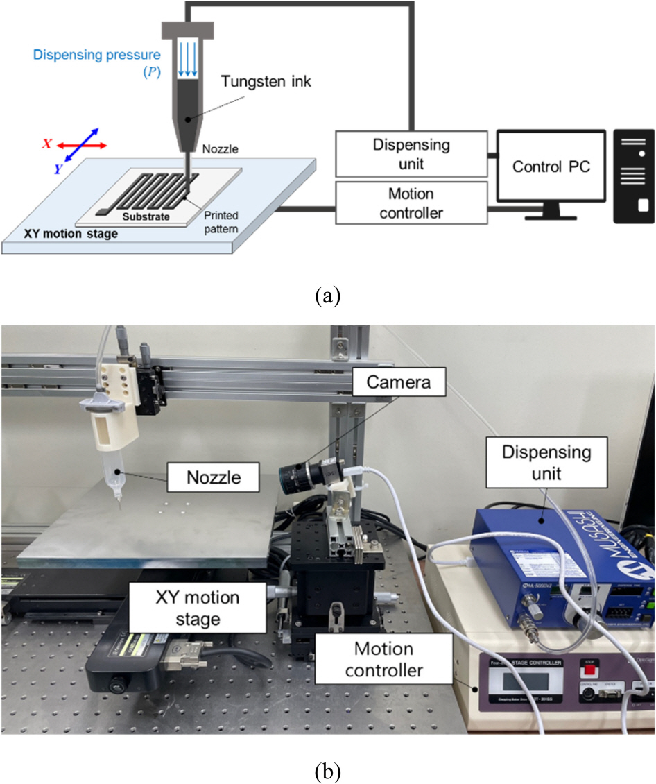
Fig. 1(a) shows a schematic of the extrusion-based dispensing system that was used in this study for DIW of planar patterns.
Fig. 1(b) presents a photo of the experimental setup. It consists of a dispensing unit (ML-5000XII, Musashi Engineering) to regulate the
P, a metallic nozzle with an inner diameter of 100 μm for dispensing tungsten ink, and an XY motion stage (OSMS26-300, Sigma Koki) to control substrate motion. The PC controls stage motion and dispensing. The syringe contained tungsten ink (Winner Technology), which was then dispensed onto alumina substrates. The writing path was segmented with a spacing of 100 μm between neighboring points, and the stage moved at a constant speed between these points. The average writing speed along the entire path was approximately 0.7 mm/s. This segmented approach is particularly advantageous in curves, where maintaining smooth motion is critical. Although momentary acceleration and deceleration may occur between neighboring points, their influence was negligible in our experiments. Further optimization of the writing motion will be studied in the future work. A camera provided real-time visual monitoring. The tungsten ink had a viscosity of approximately 50,000 mPa·s (as provided by the manufacturer), and all experiments were conducted at room temperature.
Fig. 1(a) Schematic of the extrusion-based dispensing system and (b) Photo of the experimental setup

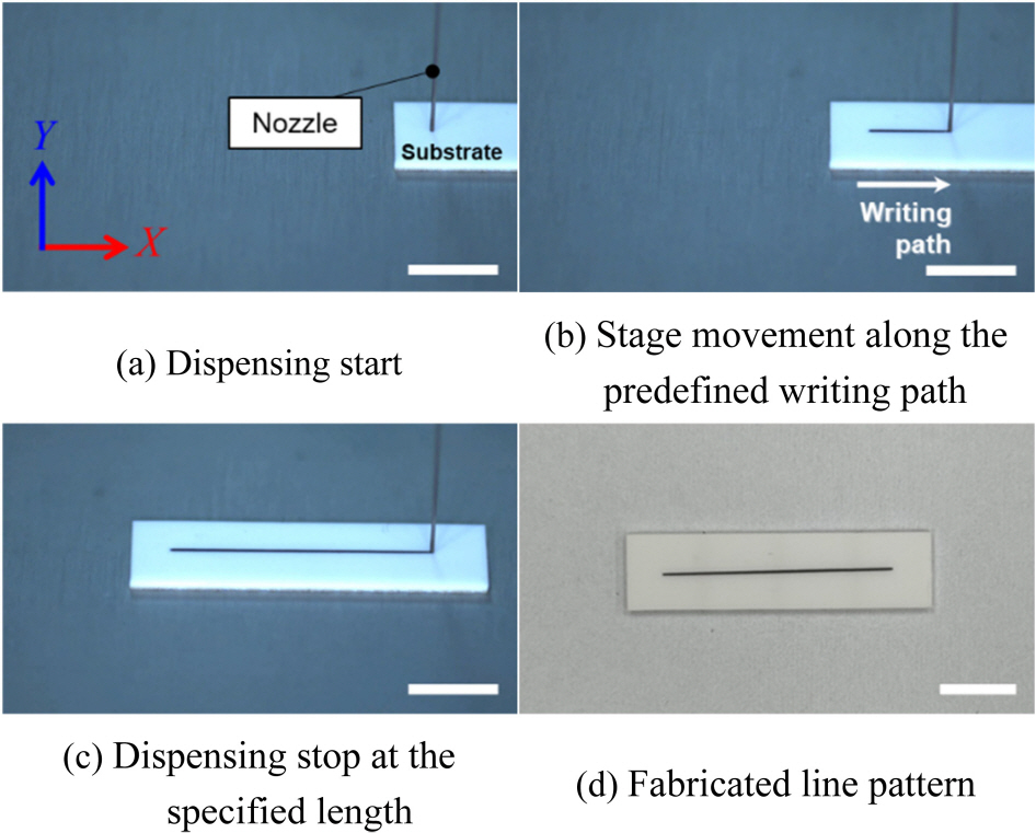
Figs. 2 shows the procedure for fabricating single lines using the extrusion-based dispensing setup shown in 1. As shown in
Fig. 2(a), the process begins with the dispensing of tungsten ink through the nozzle. The motion stage then moves along a predefined writing path (
Fig. 2(b)), and dispensing stops once it reaches the specified length (15 mm) (
Fig. 2(c)). The fabricated line pattern is shown in
Fig. 2(d).
Fig. 2Fabrication procedure of a line pattern using the extrusion-based dispensing setup. Scale bars are 5 mm in (a)-(d)

3. Results and Discussion
3.1 Effect of Dispensing Pressure on Pattern Quality
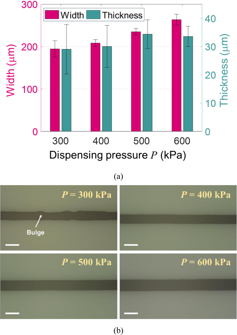
To investigate the effect of
P on the geometry of the fabricated patterns, the width and height of line patterns were measured under varying
P conditions: 300, 400, 500, and 600 kPa, as shown in Fig.3(a). Higher
P increased the ink flow rate, leading to wider and thicker line patterns.
Fig. 3(b) presents optical microscope images of line patterns fabricated under the same conditions, illustrating the influence of
P on pattern quality. At 300 kPa, bulge defects were observed, likely due to insufficient ink flow relative to the writing speed [
10,
24]. At 400 kPa, uniform patterns with a width of approximately 200 μm were obtained. Despite using a nozzle with a 100 μm inner diameter, the ink spread laterally after extrusion, increasing the pattern width to approximately 200 μm. However, by adjusting parameters such as writing speed, nozzle height above the substrate, and
P, it is expected that the pattern width can be further reduced. The influence of these parameters will be investigated in future work. Further increases in
P resulted in wider patterns, but no noticeable change in pattern quality was observed. These results indicate that control of
P is effective for adjusting pattern geometry. However, the achievable pattern width is constrained by the nozzle diameter and the rheological behavior of the ink [
25,
26], making it difficult to fabricate planar patterns wider than a line pattern. To overcome these limitations, we implemented an adjacent line overlapping strategy to modulate pattern width and fabricate planar patterns.
Fig. 3(a) Width and height measurements of line patterns fabricated under varying dispensing pressures (300, 400, 500, and 600 kPa) and (b) Optical microscope images of line patterns fabricated under the same conditions as in (a). Scale bars are 300 μm in (b)

3.2 Adhesion Test of Tungsten Patterns
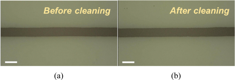
Additionally, to evaluate the adhesion of the patterns to the substrate, samples fabricated at 400 kPa were treated with ultrasonic cleaning at 40 kHz for 5 minutes.
Figs. 4(a) and
4(b) show optical microscope images of the patterns before and after cleaning. No notable changes or defects were observed, indicating sufficient adhesion of the pattern to the substrate.
Fig. 4Optical microscope images of the pattern (a) before and (b) after ultrasonic cleaning. Scale bars are 300 μm in (a) and (b)

3.3 Planar Pattern Fabrication via Adjacent Line Overlapping
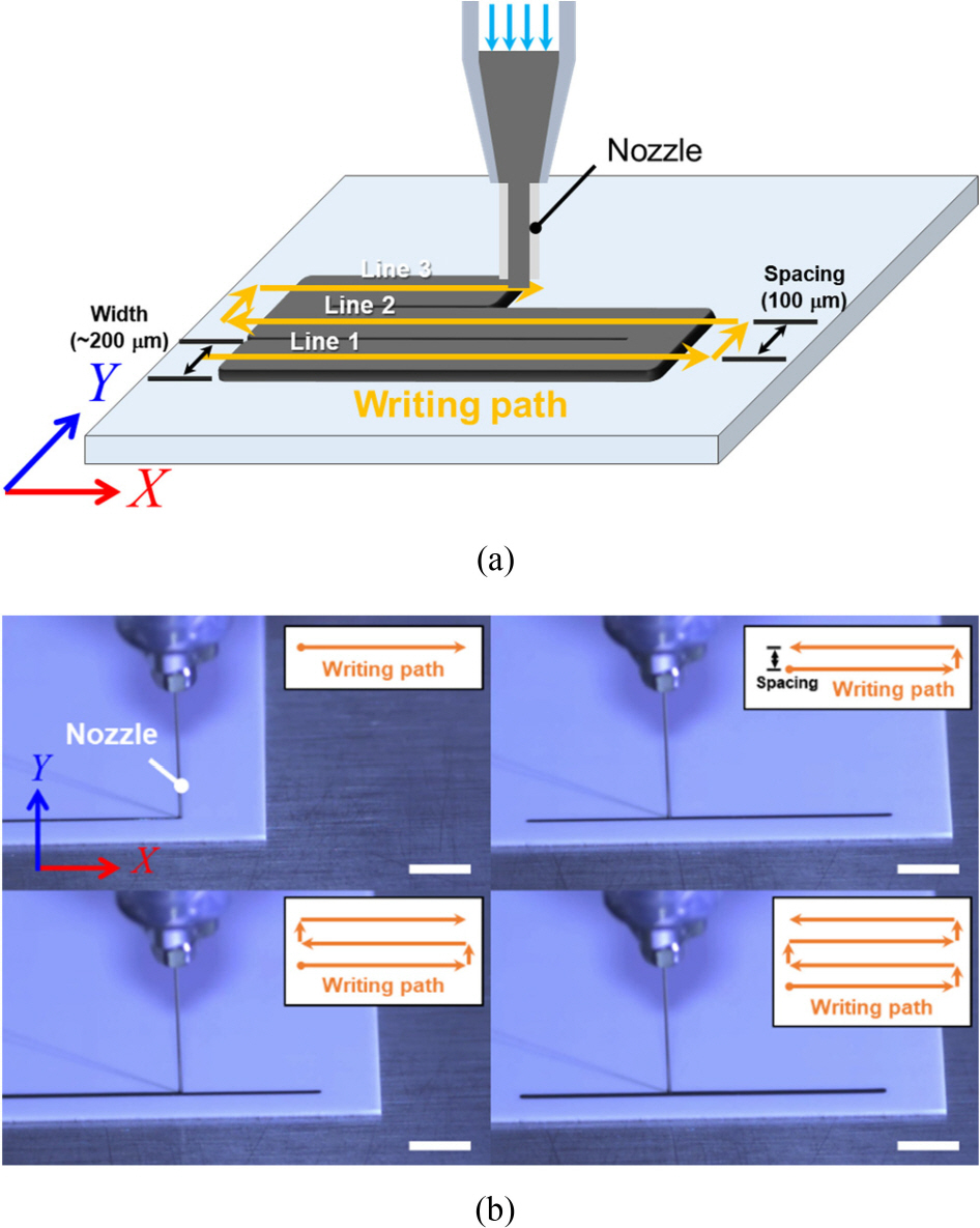
Fig. 5(a) schematically illustrates the adjacent line overlapping strategy used in this study. To fabricate planar patterns wider than a single line, several lines were sequentially written with a uniform spacing of 100 µm. Each adjacent line, approximately 200 µm in width, was written to partially overlap the previous one, forming a planar pattern with increased width.
Fig. 5(b) presents snapshot images showing the fabrication of planar patterns with a single line and up to three adjacent lines using the proposed strategy. During this process, the nozzle followed the writing path shown in the inset of
Fig. 5(b).
Fig. 5(a) Schematic of the adjacent line overlapping strategy and (b) In-situ images capturing the fabrication of planar patterns with adjacent lines. Inset in (b): schematic of the writing path used in the fabrication process. Scale bars are 5 mm in (b)

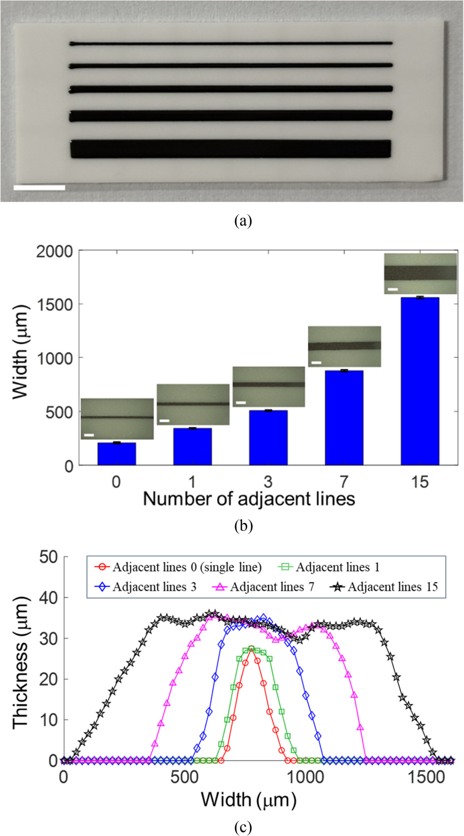
Fig. 6(a) shows planar patterns fabricated using the adjacent line overlapping strategy with varying numbers of adjacent lines: 0 (single line), 1, 3, 7, and 15. As the number of adjacent lines increased, the overall pattern width also increased, demonstrating the effectiveness of the proposed strategy.
Fig. 6(b) presents measured pattern widths and corresponding optical microscope images, confirming uniform pattern widths.
Fig. 6(c) shows the thickness profiles of the same patterns, indicating how pattern thickness changes with varying numbers of adjacent lines. The thickness increased as more lines overlapped, due to increased material deposition. To further demonstrate the versatility of this approach, we applied it to fabricate planar patterns with variable widths and complex geometries.
Fig. 6(a) Planar patterns fabricated by sequentially overlapping 0(single line), 1, 3, 7, and 15 adjacent lines, (b) Pattern widths as a function of the number of adjacent lines. Insets in (b): corresponding optical microscope images. Scale bars are 5 mm in (a), 1 mm in the insets of (b). (c) Thickness profile measurements of planar patterns fabricated with 0 (single line), 1, 3, 7, and 15 adjacent lines
3.4 Fabrication of Planar Patterns with Variable Width and Complex Geometries
To demonstrate the capability of the proposed system to fabricate patterns with variable widths, a planar pattern was designed.
Fig. 7(a) shows a design in which the pattern width varies along its length.
Fig. 7(b) presents the fabricated pattern based on this design, where the width was controlled by adjusting the number of adjacent lines. These results demonstrate that modulating the number of adjacent lines enables precise control of pattern width and provides a straightforward method for fabricating patterns with variable widths. To further demonstrate the applicability of the adjacent line overlapping strategy, planar patterns with more complex geometries were fabricated.
Figs. 8(a)-
8(c) show representative patterns, including a zigzag pattern, letter patterns, and an animal-shaped pattern. The corresponding reference images are shown as insets for comparison. These patterns include complex geometries such as curved paths, directional changes, and discontinuous features.
Fig. 7(a) Schematic diagram of a planar pattern with variable width and (b) Fabricated planar pattern with variable width. Scale bar is 5 mm in (b)
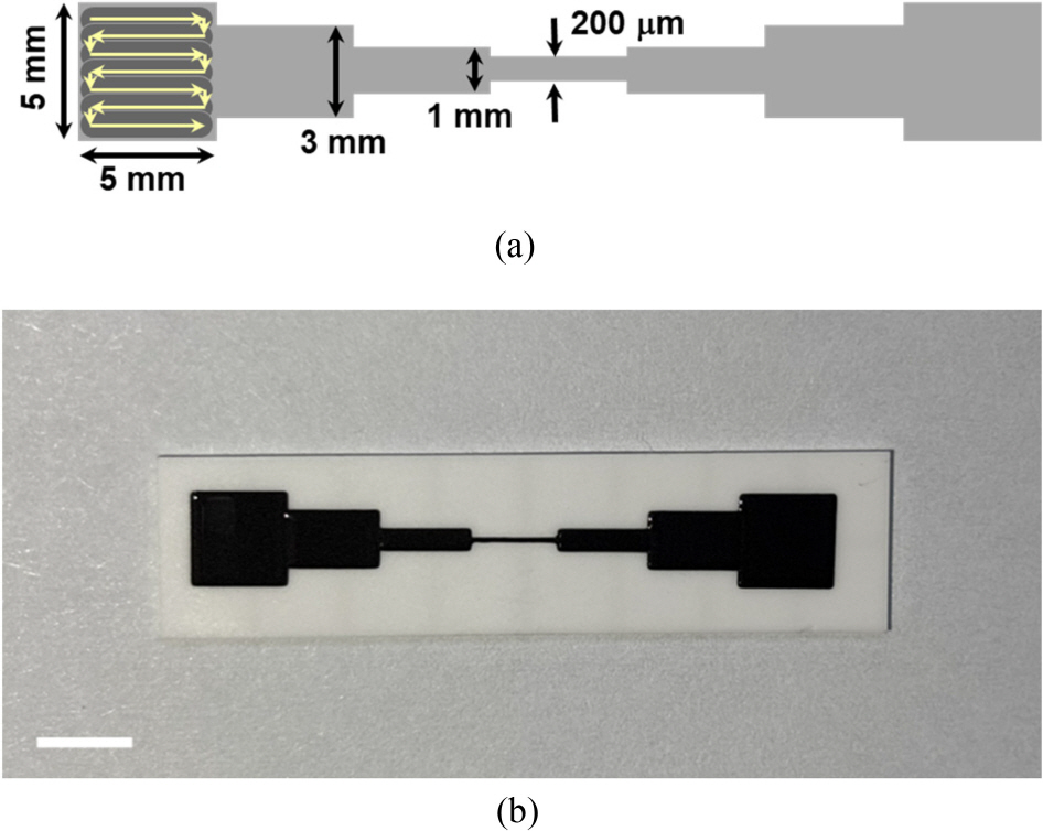
Fig. 8Representative patterns using the adjacent line overlapping strategy: (a) a zigzag pattern, (b) a letter pattern, (c) an animal-shaped pattern, and (d) in-situ images of the dispensing sequence for the discontinuous features in (c). Insets in (a)-(c): corresponding reference images. Scale bars are 5 mm in (a)-(d)
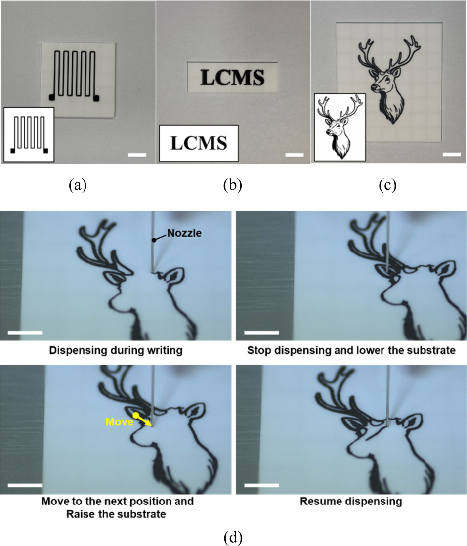
Figs. 8(d) shows snapshot images of the in-situ dispensing sequence used to fabricate the discontinuous features in 8(c). Along the writing path, dispensing was stopped at each discontinuous feature. To prevent contact between the nozzle and the previously written pattern, the substrate was lowered by 1 mm under the control of the Z motion stage (OSMS40-5ZF, Sigma Koki). The nozzle was then moved to the next position, the substrate was returned to its original height, and dispensing was resumed. The high viscosity of the tungsten ink caused a slight delay in material extrusion through the nozzle after dispensing was resumed. To address this issue, a pause of 300 ms was applied before initiating nozzle movement. We note that no clogging was observed in our experiments for 3 hours. This controlled sequence enabled the fabrication of discontinuous features without nozzle interference. These results demonstrate that the proposed system enables planar pattern fabrication with complex geometries, including variable widths, curved paths, and discontinuous features.
4. Conclusions
In summary, we introduced an extrusion-based dispensing system for the planar patterning of tungsten ink using direct ink writing. By precisely controlling the dispensing pressure (P) and substrate motion, the system enabled uniform ink deposition along predefined writing paths. To investigate the effect of P on pattern geometry, line patterns were fabricated under varying pressure conditions, and their widths and thicknesses were measured. To expand the achievable pattern width, an adjacent line overlapping strategy was implemented, wherein several lines approximately 200 µm in width were written with partial overlap. The relationship between the number of adjacent lines and the resulting pattern width was quantitatively verified. Using this approach, planar patterns with variable widths and complex geometries, such as curved paths and discontinuous features, were successfully fabricated. Discontinuous features were fabricated by lowering the substrate along the Z-axis to prevent nozzle interference. The fabricated patterns exhibited uniform quality and precision. These results demonstrate that the proposed system provides a versatile solution for fabricating planar conductive patterns with complex geometries, applicable to printed electronics and interconnects. While the system enables fabrication of patterns for such applications, the printed tungsten patterns in this study were not electrically conductive, as no sintering process was applied. Future work will focus on sintering of the pattern and evaluation of its electrical performance to verify its applicability to electronic devices. In addition, efforts will include improving pattern resolution, optimizing motion control for more complex geometries, and validating the method with other materials and substrates to broaden its applicability.
ACKNOWLEDGMENTS
This work was supported by WONIK QnC Corporation, the National Research Foundation of Korea (NRF) grant funded by the Korea government(MSIT) (No. RS-2024-00459127), the grant funded by Ministry of Trade, Industry and Energy (MOTIE, Korea) and the Korea Evaluation Institute of Industrial Technology (KEIT)(Grant No. 20017462), the Brain Korea 21 FOUR Project (Department of Aeronautics, Mechanical and Electronic Convergence Engineering, Kumoh National Institute of Technology), and the Gyeongsangbuk-do RISE (Regional Innovation System & Education) project (Specialized Industry Scale-up unit).
REFERENCES
- 1. Han, X., Lin, X., Sun, Y., Huang, L., Huo, F., Xie, R., (2024), Advancements in flexible electronics fabrication: Film formation, patterning, and interface optimization for cutting-edge healthcare monitoring devices, ACS Applied Materials & Interfaces, 16(41), 54976-55010.
- 2. Abdullah, M. R., Peng, Z., Rajendren, V. B., Ahmad, F., Shah, S. S. A., Zia, A. W., Shehzad, K., (2025), Comprehensive review of 3D/4D printing of soft materials, methods and applications, Applied Materials Today, 43, 102667.
- 3. Huang, Z., Shao, G., Li, L., (2023), Micro/nano functional devices fabricated by additive manufacturing, Progress in Materials Science, 131, 101020.
- 4. Zeng, L., Ling, S., Du, D., He, H., Li, X., Zhang, C., (2023), Direct ink writing 3D printing for high‐performance electrochemical energy storage devices: A minireview, Advanced Science, 10(32), 2303716.
- 5. Hou, Z., Lu, H., Li, Y., Yang, L., Gao, Y., (2021), Direct ink writing of materials for electronics-related applications: A mini review, Frontiers in Materials, 8, 647229.
- 6. Jo, H., Park, J. S., Lim, H. Y., Lee, G. Y., (2023), Laser sintered silver nanoparticles on the PDMS for a wearable strain sensor capable of detecting finger motion, ACS Applied Nano Materials, 6(24), 22998-23011.
- 7. Lee, G. Y., Kim, M. S., Min, S. H., Kim, H. S., Kim, H. J., Keller, R., Ihn, J. B., Ahn, S. H., (2019), Highly sensitive solvent-free silver nanoparticle strain sensors with tunable sensitivity created using an aerodynamically focused nanoparticle printer, ACS Applied Materials & Interfaces, 11(29), 26421-26432.
- 8. Qiu, M., Du, W., Zhou, S., Cai, P., Luo, Y., Wang, X., Zhao, J., (2023), Recent progress in non-photolithographic patterning of polymer thin films, Progress in Polymer Science, 142, 101688.
- 9. Huang, Q., Zhu, Y., (2019), Printing conductive nanomaterials for flexible and stretchable electronics: A review of materials, processes, and applications, Advanced Materials Technologies, 4(5), 1800546.
- 10. van Hazendonk, L. S., Vonk, C. F., van Grondelle, W., Vonk, N. H., Friedrich, H., (2024), Towards a predictive understanding of direct ink writing of graphene-based inks, Applied Materials Today, 36, 102014.
- 11. Fan, D., Lee, B., Coburn, C., Forrest, S. R., (2019), From 2D to 3D: Strain-and elongation-free topological transformations of optoelectronic circuits, Proceedings of the National Academy of Sciences, 116(10), 3968-3973.
- 12. Lee, G. S., Lee, S. H., Lee, G. Y., (2023), Tunable mechanical properties of vectran liquid crystal polymer (LCP) short fiber-reinforced soft composite, Fibers and Polymers, 24(1), 207-220.
- 13. Tuyboyov, O. V., Lee, G. S., Lee, G. Y., (2023), Multi-mode soft composite bending actuators based on glass fiber textiles interwoven with shape memory alloy wires: Development and use in the preparation of soft grippers, International Journal of Precision Engineering and Manufacturing-Green Technology, 10(5), 1263-1280.
- 14. Lee, G. Y., Lee, S. Y., (2023), Design, fabrication, and control of a rotary manipulator driven by twisted shape memory alloy (SMA) wires, Journal of the Korean Society for Precision Engineering, 40(8), 665-673.
- 15. Zhu, Y. M., Tang, J., Jin, X., Pan, T. R., Chang, Y., Yang, Z. G., (2020), Additive preparation of conductive circuit based on template transfer process using a reusable photoresist, ACS Applied Materials & Interfaces, 12(6), 7679-7689.
- 16. You, K., Wang, Z., Lin, J., Guo, X., Lin, L., Liu, Y., Huang, W., (2024), On‐demand picoliter‐level‐droplet inkjet printing for micro fabrication and functional applications, Small, 20(46), 2402638.
- 17. Wu, G., Wu, L., Zhang, H., Wang, X., Xiang, M., Teng, Y., Gao, L., (2024), Research progress of screen-printed flexible pressure sensor, Sensors and Actuators A: Physical, 115512.
- 18. Gupta, V. K., Kumar, N., (2024), Direct ink writing of copper-based highly conductive tracks on flexible substrate for electronic applications, Materials Letters, 372, 137008.
- 19. Zhang, P., Sun, Q., Fang, S., Guo, H., Liu, K., Zhang, L., Wang, M., (2024), Fabrication of nano copper highly conductive and flexible printed electronics by direct ink writing, ACS Applied Materials & Interfaces, 17(1), 1847-1860.
- 20. Hossain, M. J., Tabatabaei, B. T., Kiki, M., Choi, J. W., (2025), Additive manufacturing of sensors: A comprehensive review, International Journal of Precision Engineering and Manufacturing-Green Technology, 12(1), 277-300.
- 21. Romario, Y. S., Bhat, C., Ramezani, M., Jiang, C. P., (2025), Marine waste management of oyster shell waste as reinforcement for clay additive manufacturing components, International Journal of Precision Engineering and Manufacturing-Green Technology, 12(1), 117-134.
- 22. Park, Y. G., Yun, I., Chung, W. G., Park, W., Lee, D. H., Park, J. U., (2022), High‐resolution 3D printing for electronics, Advanced Science, 9(8), 2104623.
- 23. Zhao, Z., Liu, W., Liu, H., (2025), Flexible and durable direct ink writing 3D-printed conductive fabrics for smart wearables, ACS Omega, 10(14), 14138-14149.
- 24. Jiang, Y., Wang, X., Plog, J., Yarin, A. L., Pan, Y., (2021), Electrowetting-assisted direct ink writing for low-viscosity liquids, Journal of Manufacturing Processes, 69, 173-180.
- 25. Lewis, J. A., (2006), Direct ink writing of 3D functional materials, Advanced Functional Materials, 16(17), 2193-2204.
- 26. Abas, M., Salman, Q., Khan, A. M., Rahman, K., (2019), Direct ink writing of flexible electronic circuits and their characterization, Journal of the Brazilian Society of Mechanical Sciences and Engineering, 41, 1-11.
Biography
Min-Hyeong Lee
M. S. candidate in the Department of Mechanical Engineering, Kumoh National Institute of Technology. His research interests are additive manufacturing, robotics, and vibration.
Seung-Hyeon Choi
M. S. candidate in the Department of Mechanical Engineering, Kumoh National Institute of Technology. Her research interests are additive manufacturing and robotics.
Jae-Wook Yu
M. S. candidate in the Department of Mechanical Engineering, Kumoh National Institute of Technology. His research interests are additive manufacturing and robotics.
Ji-Su Park
M. S. candidate in the Department of Mechanical Engineering, Kumoh National Institute of Technology. Her research interests are additive manufacturing and machine vision.
Hyuk-Chun Kwon
Team leader in Materials R&D Center, WONIK QnC Corporation. His research interests are ceramic materials and electronic applications.
Ho-Chang Lee
Manager in Materials R&D Center, WONIK QnC Corporation. His research interests are ceramic materials and electronic applications
Seong-Uk Oh
Manager in Materials R&D Center, WONIK QnC Corporation. His research interests are ceramic materials and electronic applications
Seung-Gon Choi
Manager in Materials R&D Center, WONIK QnC Corporation. His research interests are ceramic materials and electronic applications
In-Gu Choi
Manager in Materials R&D Center, WONIK QnC Corporation. His research interests are ceramic materials and electronic applications
Gil-Yong Lee
Associate Professor in the Department of Mechanical Engineering, Kumoh National Institute of Technology. His research interests are integrated manufacturing system, sensors/actuators, composites, vibration, control, and additive manufacturing.