ABSTRACT
The practical application of Raman spectroscopy is often constrained by its low signal sensitivity, particularly for low-concentration liquid samples. This study introduces a straightforward platform that enhances Raman signals by physically concentrating analytes, providing an alternative to complex substrate fabrication and chemical treatments. We employed a femtosecond pulse laser to create functional micro-grid patterns on a silicon (Si) substrate. This laser process induces localized ablation and simultaneous oxidation, resulting in three-dimensional, hydrophilic microstructures of non-stoichiometric silicon oxide (SiO2-x). These grid structures effectively confine aqueous sample droplets through a pinning effect, functioning as a microwell array that traps and concentrates suspended polystyrene (PS) particles. This physical concentration mechanism achieved a notable signal enhancement, with a maximum factor of 5.2 for PS particles, without the need for sample dehydration. This work presents a simple, cost-effective, and highly reproducible alternative to conventional SERS for analyzing low-concentration liquid samples, demonstrating strong potential for integration into microfluidic systems.
-
KEYWORDS: Raman spectroscopy, Femtosecond laser processing, Surface patterning, Signal enhancement, Physical concentration
-
KEYWORDS: 라만 분광법, 펨토초 레이저 가공, 표면 패터닝, 신호 증강, 물리적 농축
NOMENCLATURE
PS = Polystyrene
1. Introduction
Raman spectroscopy is a powerful analytical technique that provides non-destructive structural information on materials by detecting the unique vibrational modes of molecules [
1,
2]. It plays a pivotal role in a wide range of fields, including materials science, chemistry, and life sciences, offering the distinct advantage of high selectivity in identifying specific components within complex mixtures. The fundamental principle of Raman spectroscopy is based on the Raman effect, where monochromatic light (laser) is inelastically scattered by molecules [
3]. While most photons are scattered at the same frequency as the incident light (Rayleigh scattering), an extremely small fraction—approximately one in ten million—is scattered with a shifted frequency due to changes in the vibrational energy of the molecules [
3].
This mechanism, which detects changes in the polarizability of molecular bonds, distinguishes it from Fourier-transform infrared (FTIR) spectroscopy, which measures changes in the dipole moment [
4]. This characteristic allows for the effective analysis of materials that are difficult or impossible to observe with FTIR, such as homonuclear bonds like carbon-carbon (C-C) and sulfursulfur (S-S), as well as particles in polar solvents like water [
5,
6]. These unique advantages have established Raman spectroscopy as an indispensable tool for applications such as monitoring chemical synthesis, crystallization processes, and biocatalysis.
Despite its inherent strengths, Raman spectroscopy faces a fundamental limitation: the extremely low probability of the Raman effect. The intensity of Raman scattering is typically 10-6 to 10-8 times weaker than that of Rayleigh scattering [
7]. Consequently, when analyzing low-concentration samples, the faint signal can be obscured by background noise, making precise analysis challenging. This low sensitivity is a major obstacle to the practical application of the technology, particularly for detecting trace amounts of biomolecules or environmental pollutants.
The most extensively studied technique to overcome this issue is Surface-Enhanced Raman Scattering (SERS) [
1,
2]. SERS utilizes the phenomenon of Localized Surface Plasmon Resonance (LSPR), which occurs on the surface of noble metal nanostructures, such as gold (Au) or silver (Ag). This resonance can induce a powerful electromagnetic enhancement, amplifying the Raman signal of nearby analytes by factors of 106 or more, enabling detection even at the single-molecule level [
8,
9]. As a result, SERS has garnered significant attention as a revolutionary analytical method in fields requiring high-sensitivity analysis, including biosensing, medical diagnostics, and environmental monitoring.
However, despite its high sensitivity, SERS technology often requires complex and costly nano-fabrication processes [
10]. More importantly, issues of signal reproducibility and substrate uniformity remain unresolved. The massive enhancement in SERS is critically dependent on how efficiently analytes are positioned within nanoscale “hot spots.” Achieving uniform control over the density and distribution of these hot spots over large areas is a formidable engineering challenge [
11]. Inefficient adsorption of analytes onto hot spots or non-uniform hot spot density leads to poor signal reproducibility, which undermines the reliability of analytical results. These practical limitations constrain the real-world application of SERS despite its high sensitivity. Against this backdrop, this study aims to develop a simple yet reproducible platform for Raman signal enhancement, proposing a new approach that is distinct from conventional electromagnetic/chemical mechanisms.
This research introduces a new paradigm that focuses on the physical concentration of analytes to enhance Raman signals, utilizing femtosecond laser micro-fabrication [
12]. A femtosecond laser is characterized by an extremely short pulse duration (typically 10
-15-10
-13 s). The 400 fs (4 × 10
-13 s) laser used in this study possesses an interaction time that is comparable to or shorter than the thermal diffusion time of materials (typically 10
-12-10
-9 s). This unique characteristic enables precise material removal (ablation) via non-linear, non-thermal processes, minimizing the heat-affected zone (HAZ) [
12]. When a femtosecond laser beam is focused on a silicon (Si) substrate, its extremely high peak power induces non-linear optical phenomena such as multi-photon absorption and tunneling ionization [
12]. This process generates a high density of free electrons, which transfer energy to the lattice atoms, transitioning the material into a plasma state. The subsequent expansion of this plasma results in precise material removal, known as ablation. Simultaneously, the ultra-hot Si surface reacts with atmospheric oxygen (O) to form a layer of non-stoichiometric silicon oxide (SiO
2-x), creating a three-dimensional microstructure.
The ultimate goal of this study is to fabricate a functional microgrid pattern on a Si substrate using femtosecond laser direct writing and to utilize it as a platform for physically trapping and concentrating suspended particles in liquid samples.
Unlike approaches that rely on noble metal nanoparticles or complex chemical treatments, our approach solely utilizes the physical structuring of the surface and the surface chemistry modification induced by laser oxidation [
10,
12]. This presents a new paradigm for enhancing Raman signals by physically concentrating the analyte within the laser interrogation volume. This work explores the potential of this simple and reproducible methodology.
2. Experimental Methods
A femtosecond pulse laser-based surface patterning system was used for the fabrication of SiO
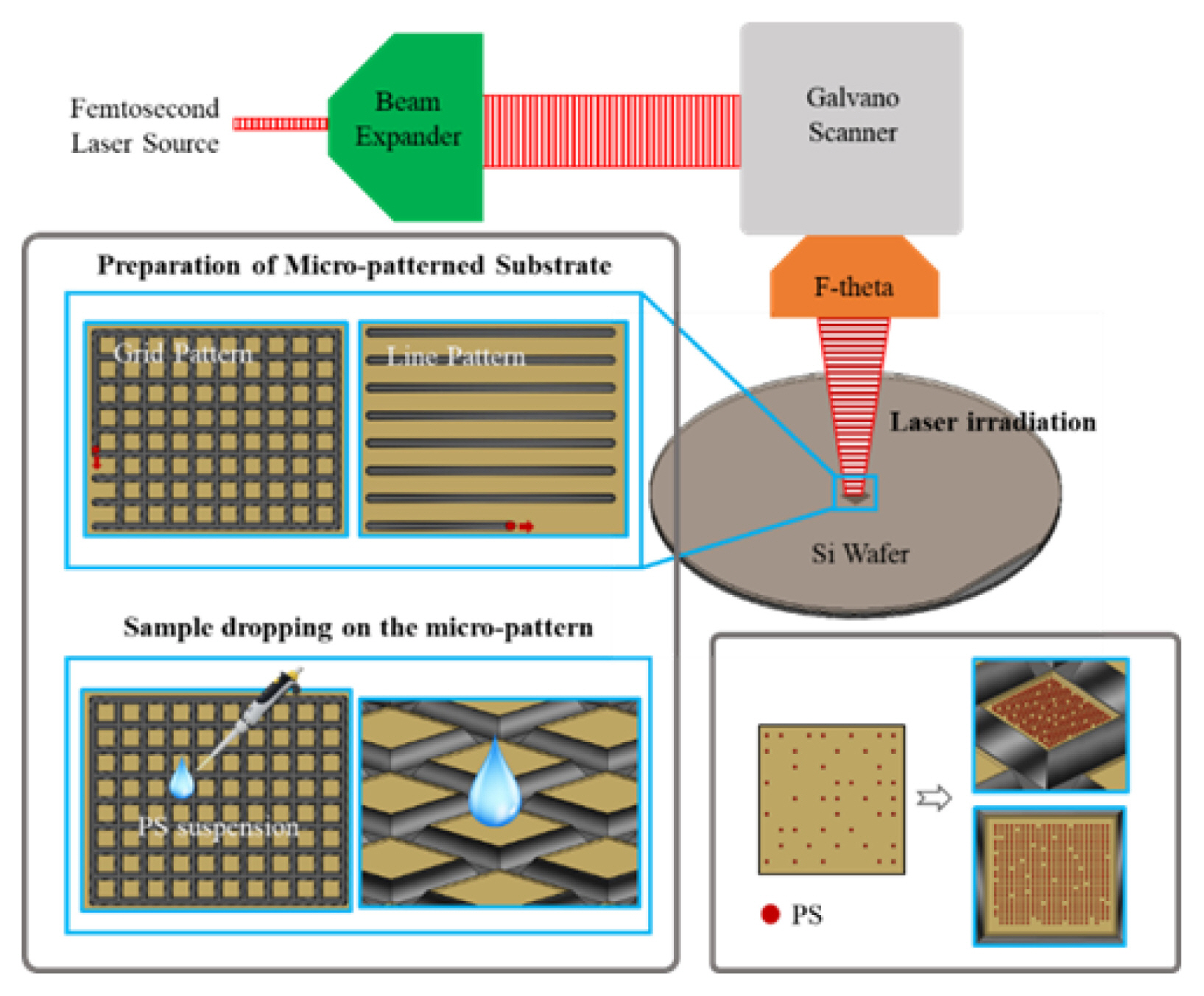
2-x/Si grid patterns. The laser source had a central wavelength of 1,040 nm, a pulse duration of 400 fs, and a repetition rate of 200 kHz. The laser beam was expanded, directed by a galvano scanner, and precisely focused onto the Si wafer surface through an F-theta lens, as shown in
Fig. 1. To optimize the laser processing parameters, the average laser power was fixed at 3.75 W, while the scan speed was systematically varied from 2.5 to 200 mm/sec. The beam diameter on the silicon wafer was approximately 30 μm. The laser fluence (F) was calculated using F = P
avg/(f ·A), where P
avg is the average laser power, f is the pulse repetition rate, and A is the beam area. Based on these parameters, the resulting fluence was approximately 2.65 J/cm
-2. A grid structure composed of square unit cells measuring 100 μm × 100 μm was fabricated, as illustrated in
Fig. 1, to create a microstructured surface designed to confine PS particles.
An aqueous suspension of PS particles with an average diameter of 1.6 μm at a concentration of 2.5% (w/v) was used as a standard sample to evaluate the Raman signal enhancement effect. The prepared PS suspension was dropped onto the fabricated grid-patterned substrate and a non-patterned bare Si substrate (for comparison), and Raman spectra were acquired immediately in the liquid state without a drying process. The surface morphology and microstructure of the patterns were observed using Field Emission Scanning Electron Microscopy (FE-SEM, Quanta 200 FEG, FEI Company). The 3D surface profile (ridge height, groove depth) was quantitatively analyzed with an Alpha-Step surface profiler (P-16, KLA-Tencor). Here, the groove depth is defined as the maximum vertical distance from the original Si wafer surface (baseline) down to the bottom of the ablated channel. The ridge height is defined as the maximum vertical distance from the original Si wafer surface up to the peak of the resolidified material (ridge) adjacent to the groove. The chemical composition of the patterned surface was analyzed by Energy-Dispersive X-ray Spectroscopy (SEM-EDS, Quanta 200 FEG, FEI Company) to quantify the atomic percentages of oxygen and silicon. The analysis was specifically focused on the newly formed ridge structures of the line patterns, which are the primary sites of laser-induced oxidation. Raman signals were measured using a micro-Raman spectrometer (NRS-5100, JASCO) equipped with a laser of 633 nm wavelength.
3. Results and Discussion
In femtosecond laser processing, the scan speed is a critical parameter that determines the total energy dose per unit area, or fluence.
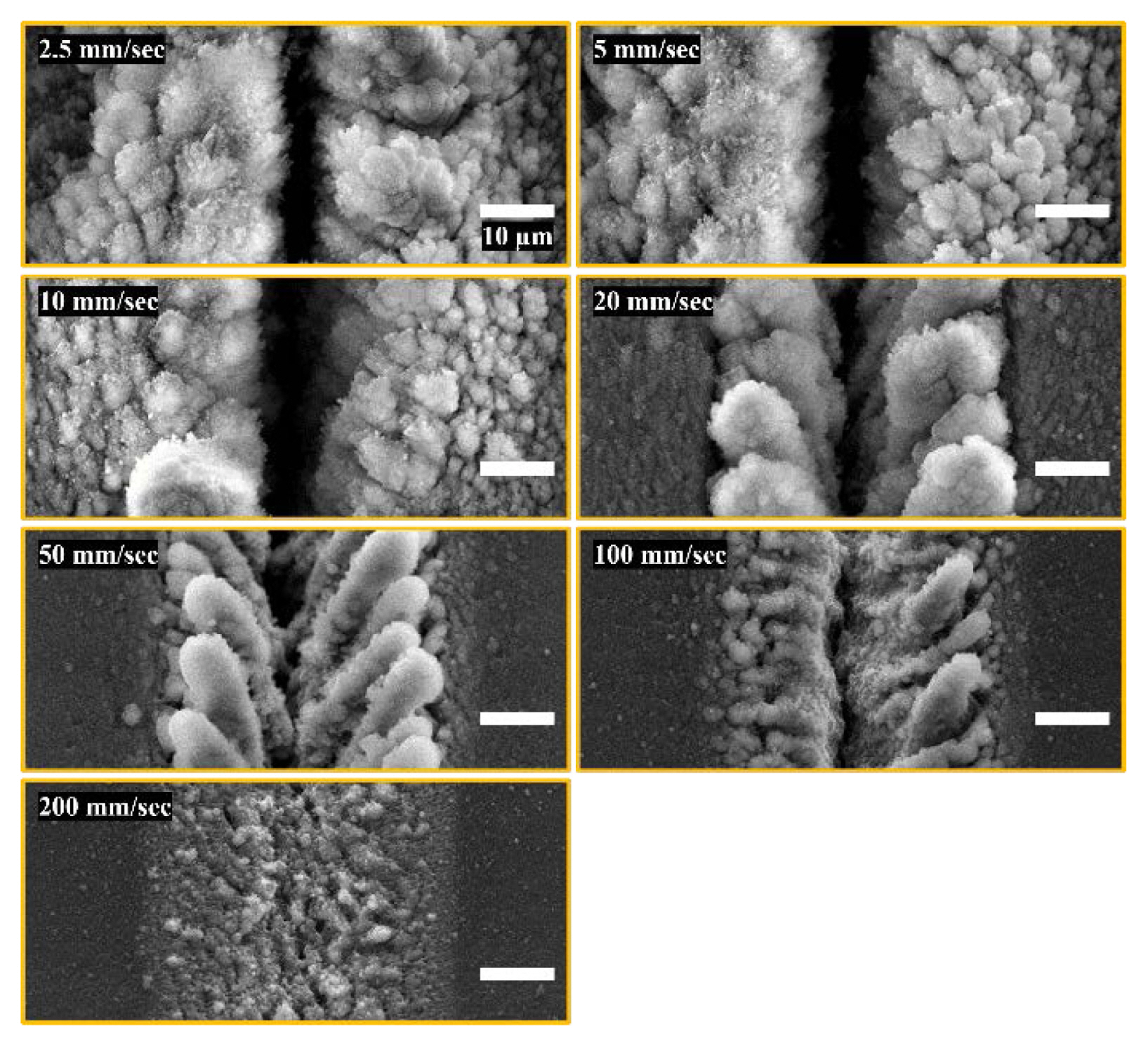
Figs. 2 and
3 clearly illustrate the changes in the surface morphology and microstructure of the line patterns as a function of scan speed. At a very low scan speed of 2.5 mm/sec, a “heat accumulation effect” occurred, where excessive laser energy was deposited onto the substrate. This led to uncontrolled over-melting and irregular ablation, resulting in poorly defined patterns and a significant amount of debris. In contrast, as the scan speed increased from 5 mm/sec to 50 mm/sec, a balance was achieved between material removal by ablation and the resolidification of molten silicon, leading to the formation of uniform and well-defined line patterns.
Notably, the ridges formed in this regime exhibited porous nano/microstructures, similar to Laser-Induced Periodic Surface Structures (LIPSS). These structures are formed as the molten silicon rapidly reacts with atmospheric oxygen and resolidifies, and they can influence surface properties that contribute to subsequent Raman signal enhancement.
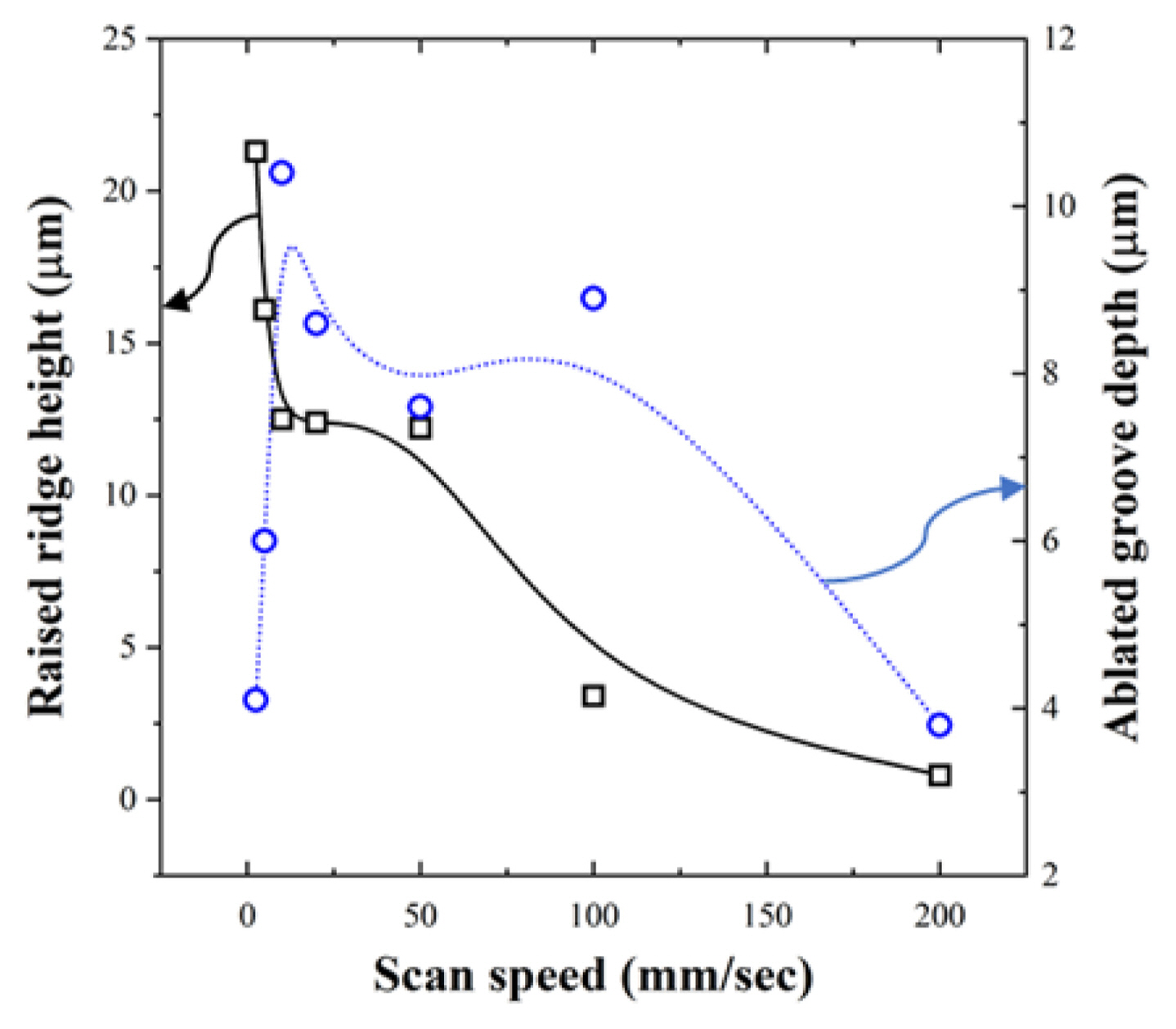
However, as the scan speed increased beyond 100 mm/sec, the fluence per unit area dropped below the ablation threshold, leading to inefficient material removal and the formation of shallow, indistinct patterns. The quantitative analysis of the pattern's cross-sectional profile as a function of scan speed is shown in
Fig. 4.
The groove depth reached a maximum of approximately 10.5 μm at 10 mm/sec, whereas the ridge height was highest at approximately 21 μm at 5 mm/sec. This suggests that the physical mechanisms governing ridge height and groove depth are subtly different. The groove depth is primarily proportional to the amount of material directly removed by laser ablation. The 10 mm/sec condition is presumed to be most efficient for energy concentration leading to material removal. In contrast, the ridge height is determined by the amount of molten material displaced to the periphery by plasma pressure and subsequently resolidified. The 5 mm/sec condition likely provided the most favorable conditions for forming a high ridge by creating a sufficient molten pool and strong plasma pressure. At 10 mm/sec, the energy may have been more effectively used for material removal, leaving less molten material to form ridges.
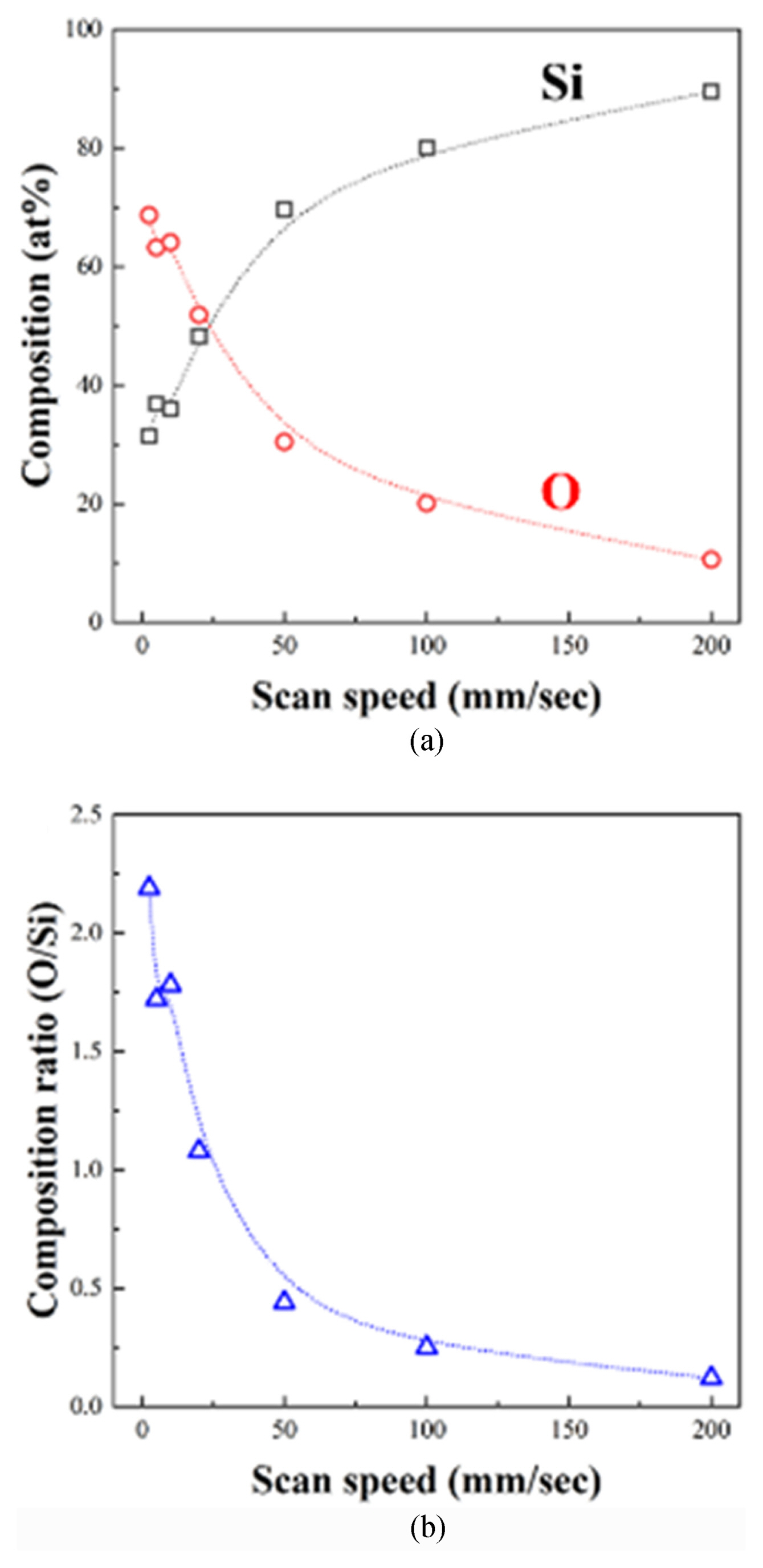
The SEM-EDS analysis of the pattern's chemical composition, shown in
Fig. 5, clearly demonstrates the laser-induced oxidation reaction. As the scan speed decreased, meaning a longer interaction time between the laser and the substrate, the atomic percentage of oxygen (O) on the surface gradually increased. At the low scan speed of 2.5 mm/sec, the O/Si ratio reached approximately 2.2, a composition close to stoichiometric SiO
2, indicating that a sufficient oxidation reaction had occurred on the hot Si surface. As the scan speed increased, the time available for oxidation was insufficient, causing the O/Si ratio to decrease sharply, reaching a low value of 0.13 at 200 mm/sec. These data signify that by controlling the femtosecond laser processing parameters, not only the physical morphology but also the surface chemistry (e.g., hydrophilicity/hydrophobicity) can be precisely tuned. It is well-established that silicon oxide is inherently more hydrophilic than bare silicon. Therefore, the confirmed formation of this SiO
2-x layer (validated by
Fig. 5) is the key factor that induces surface hydrophilicity, which in turn effectively confines the aqueous sample droplet within the grid pattern.
The scan speed thus serves as a multifunctional process parameter that simultaneously controls the 3D geometry and surface chemistry of the pattern, which is a core design element of this Raman signal enhancement platform. The primary goal of this study is to fabricate a functional grid for effective droplet pinning, which demands both a high physical barrier to prevent spreading and a hydrophilic surface chemistry to attract the liquid. Analyzing the data from
Figs. 4 and
5, the 5 mm/sec condition represents the optimal balance that satisfies both key requirements. Specifically, 5 mm/sec provides the highest ridge height (~21 μm) of all conditions (
Fig. 4), creating the most effective physical barrier. Simultaneously, it produces a high O/Si ratio of 1.75 (
Fig. 5), ensuring the surface is sufficiently hydrophilic to induce a Wenzel state. In contrast, the 10 mm/sec condition offered a lower ridge height, while the 2.5 mm/sec condition resulted in poor pattern fidelity due to excessive heat accumulation. Based on these comprehensive optimization results, a 100 × 100 μm
2 grid pattern fabricated at a scan speed of 5 mm/sec was used for the Raman signal enhancement experiment. As shown in
Fig. 6, the hydrophilic SiO
2-x ridges formed by laser processing induce a “pinning effect” that prevents the aqueous sample droplet from spreading, confining it within the grid [
13]. This observed pinning is the direct result of the surface adopting a Wenzel wetting state, which is described by the Wenzel wetting model that explains the interaction between a liquid and a hydrophilic, micro-structured surface [
14]. Unlike the Cassie-Baxter model, which describes a liquid droplet suspended on top of structures on a superhydrophobic surface, the Wenzel model describes a state where the liquid penetrates the voids between microstructures on a hydrophilic surface, making uniform contact. The SiO
2-x ridges are hydrophilic, and the deep grooves act as voids. Therefore, the liquid sample spreads over the grid pattern and becomes trapped within the grooves, corresponding to a Wenzel state.
This state increases the contact area of the liquid droplet, suppressing its outward spreading and effectively concentrating the suspended particles within the grid, which acts as a “microwell” array.
The data in
Fig. 7 and
Table 1 quantitatively validate this physical concentration effect. The Raman spectrum measured on the grid pattern exhibited significantly higher intensities for all characteristic peaks of PS compared to the spectrum from the non-patterned Si substrate. Specifically, the signal intensity was enhanced by a factor of 4.3 for the aromatic ring breathing mode (~1,001 cm
-1) and up to 5.2 for the C-H bending mode (~1,030 cm
-1). The Raman spectra of PS obtained from the patterned and non-patterned regions revealed an intensity ratio of 5.2, indicating that the observed signal increase originates from a physical concentration mechanism rather than an electromagnetic effect.
While the Raman intensity ratio of 5.2 is relatively modest compared to that of SERS technology (>106), this value does not diminish the academic merit of this study. The massive enhancement of SERS is based on complex electromagnetic mechanisms like plasmon resonance of noble metal nanoparticles, which entails drawbacks such as complex processing, high cost, and reproducibility issues. In contrast, the 5.2-fold enhancement achieved in this study was accomplished purely by the physical concentration of the liquid sample by the grid pattern, without any such complex pretreatments or expensive noble metal nanostructures. This demonstrates a new possibility for improving Raman sensitivity through a simple and reproducible method. Therefore, this factor of 5.2 serves as a crucial “proof-of-concept” that validates the novel concept of this study: a Raman signal enhancement platform based on physical concentration.
4. Conclusion
In this study, we successfully designed and fabricated a functional SiO2-x/Si micro-grid pattern based on the physical concentration of particles in a liquid sample, utilizing femtosecond laser direct writing technology. By precisely controlling the single process parameter of laser scan speed, we simultaneously optimized the 3D morphology and surface chemistry of the pattern. Specifically, at a scan speed of 5 mm/sec, we achieved a pattern with the most pronounced ridge structure and a high degree of oxidation, which played a crucial role in inducing a “pinning effect” that suppressed the spreading of liquid droplets and effectively concentrated particles within the grid.
This physical concentration mechanism is in perfect agreement with the Wenzel wetting model, which describes the interaction of a liquid with a hydrophilic micro-structured surface. Through this effect, the Raman signal intensity of PS particles measured in the liquid state without any drying process was enhanced by up to a factor of 5.2 compared to a non-patterned Si substrate.
In conclusion, this study presents a simple and reproducible methodology that can significantly improve the sensitivity of Raman analysis for low-concentration liquid samples without complex chemical pre-treatment processes. This enhances the feasibility of applying trace analysis techniques in the field and is expected to expand its utility through integration with microfluidics and lab-on-a-chip systems. The physical concentration-based platform presented in this study offers a practical and cost-effective approach for trace analysis, marking an important milestone for the practical application of Raman spectroscopy. While this study utilized PS particles as a proof-of-concept, the analyte-agnostic nature of the physical concentration mechanism suggests strong potential for enhancing signals from other, weaker-scattering analytes, such as various biomolecules or environmental pollutants. Validating this broader applicability will be a key focus of our future investigations.
FOOTNOTES
-
ACKNOWLEDGEMENT
This work was supported by the Korea Institute of Energy Technology Evaluation and Planning (KETEP) and the Ministry of Trade, Industry & Energy (MOTIE) of the Republic of Korea (No. RS-2024-00400653).
Fig. 1Schematic diagram of femtosecond pulse laser-based SiO2-x/Si line and grid pattern formation for the enhancement of Raman intensity of PS particles in PS suspension

Fig. 2SEM surface morphology of SiO2-x/Si patterns according to the pulse laser scan speed
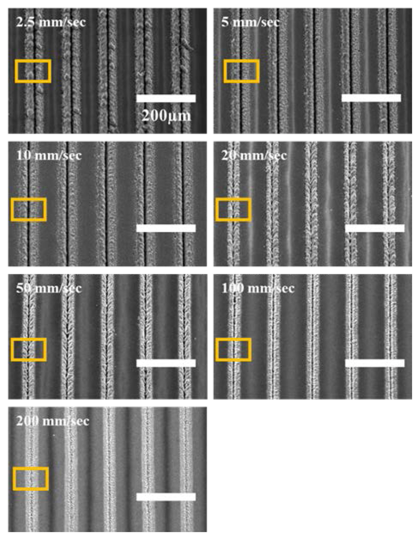
Fig. 3Microstructure of SiO2-x/Si patterns as a function of the pulse laser scan speed

Fig. 4Ridge height and groove depth of SiO2-x/Si patterns analyzed by Alpha-Step depending on the pulse laser scan speed

Fig. 5(a) Composition distribution and (b) O/Si composition ratio of SiO2-x/Si line patterns analyzed by SEM-EDS according to the pulse laser scan speed

Fig. 6Surface morphology of PS particles distributed in the center and edge regions of a 100 × 100 μm2 grid pattern
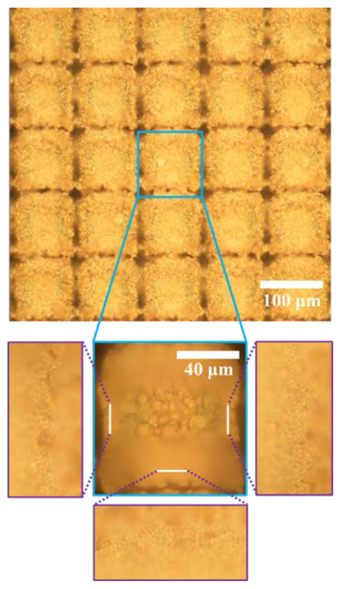
Fig. 7Raman spectra analyzed on a 100 × 100 μm2 grid pattern and a non-patterned Si substrate
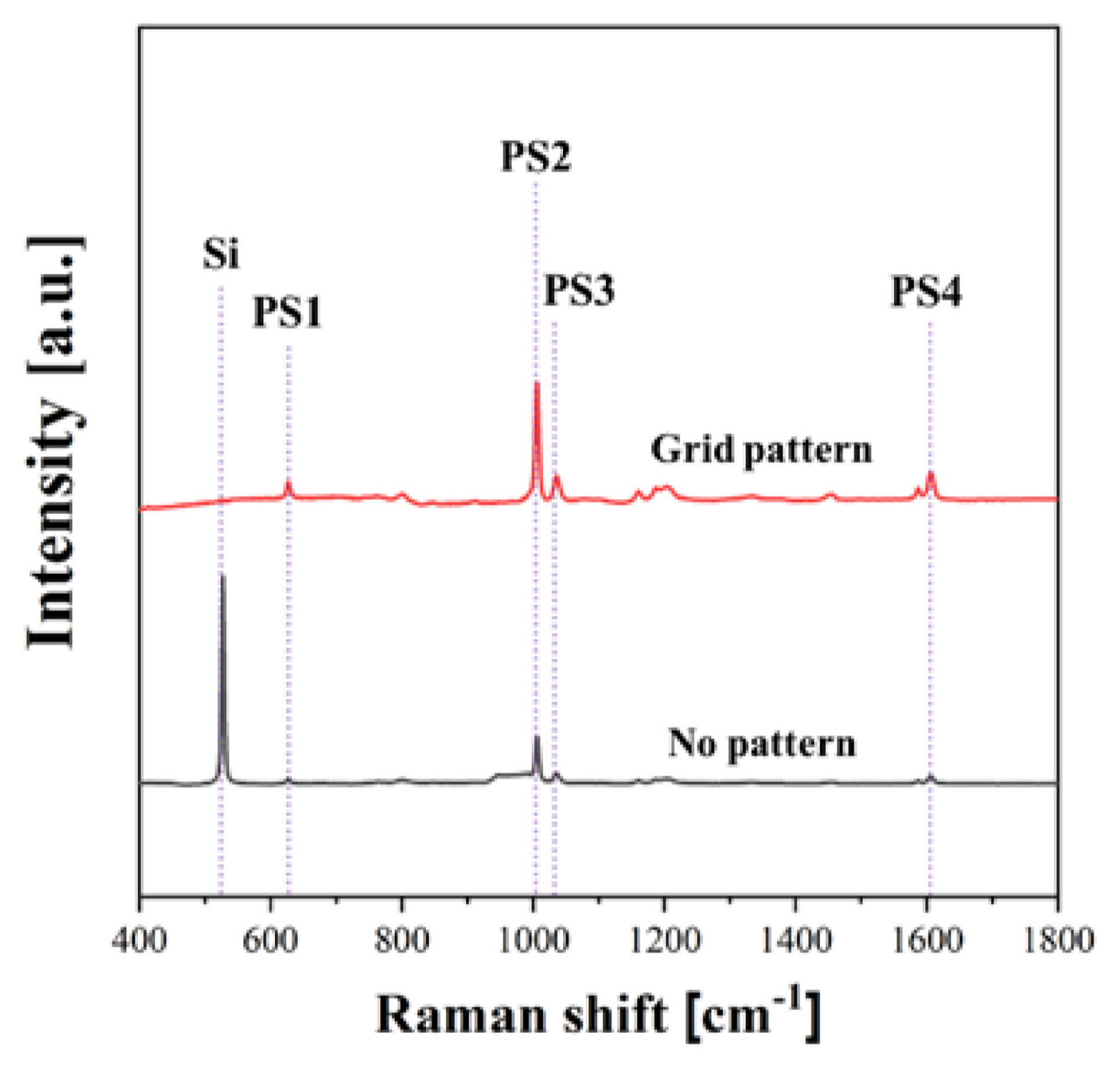
Table 1Vibration modes and intensity ratios corresponding to the Raman scattering peaks
Table 1
|
Scattering peak [cm−1] |
Assigned material |
Vibration mode |
Intensity ratio [IG/IN] |
|
520 |
c-Si |
First-order optical phonon |
- |
|
~620 |
Polystyrene (PS1) |
Ring deformation |
3.0 |
|
~1,001 |
Polystyrene (PS2) |
Aromatic ring breathing |
4.3 |
|
~1,030 |
Polystyrene (PS3) |
C-H bending |
5.2 |
|
~1,602 |
Polystyrene (PS4) |
C = C aromatic ring stretching |
2.5 |
REFERENCES
- 1. Fleischmann, M., Hendra, P. J., McQuillan, A. J., (1974), Raman spectra of pyridine adsorbed at a silver electrode, Chemical Physics Letters, 26(2), 163-166.
- 2. Jeanmaire, D. L., Van Duyne, R. P., (1977), Surface Raman spectroelectrochemistry: Part i. Heterocyclic, aromatic, and aliphatic amines adsorbed on the anodized silver electrode, Journal of electroanalytical chemistry and interfacial electrochemistry, 84(1), 1-20.
- 3. Han, X. X., Rodriguez, R. S., Haynes, C. L., Ozaki, Y., Zhao, B., (2021), Surface-enhanced raman spectroscopy, Nature Reviews Methods Primers, 1(1), 87.
- 4. Diebold, E. D., Mack, N. H., Doorn, S. K., Mazur, E., (2009), Femtosecond laser-nanostructured substrates for surface-enhanced Raman scattering, Langmuir, 25(3), 1790-1794.
- 5. Chang, H.-W., Tsai, Y.-C., Cheng, C.-W., Lin, C.-Y., Lin, Y.-W., Wu, T.-M., (2011), Nanostructured Ag surface fabricated by femtosecond laser for surface-enhanced Raman scattering, Journal of Colloid and Interface Science, 360(1), 305-308.
- 6. Zalloum, O. H., Parrish, M., Terekhov, A., Hofmeister, W., (2010), An amplified femtosecond laser system for material micro-/nanostructuring with an integrated Raman microscope, Review of Scientific Instruments, 81(5.
- 7. Varkentina, N., Dussauze, M., Royon, A., Ramme, M., Petit, Y., Canioni, L., (2015), High repetition rate femtosecond laser irradiation of fused silica studied by Raman spectroscopy, Optical Materials Express, 6(1), 79-90.
- 8. Hamad, S., Bharati Moram, S. S., Yendeti, B., Podagatlapalli, G. K., Nageswara Rao, S., Pathak, A. P., Mohiddon, M. A., Soma, V. R., (2018), Femtosecond laser-induced, nanoparticle-embedded periodic surface structures on crystalline silicon for reproducible and multi-utility SERS platforms, Acs Omega, 3(12), 18420-18432.
- 9. Bai, S., Sugioka, K., (2021), Recent advances in the fabrication of highly sensitive surface-enhanced raman scattering substrates: Nanomolar to attomolar level sensing, Light: Advanced Manufacturing, 2(2), 186-210.
- 10. Huang, C., Li, H., Zhang, X., (2024), Direct writing of SERS substrates using femtosecond laser pulses, ACS Omega, 9(35), 37188-37196.
- 11. Hu, Y., Hu, Y., Wang, Z., Yong, J., Xiong, W., Wu, D., Xu, S., (2024), Efficient concentration of trace analyte with ordered hotspot construction for a robust and sensitive SERS platform, International Journal of Extreme Manufacturing, 6(3), 035505.
- 12. Stuart, B. C., Feit, M. D., Herman, S., Rubenchik, A. M., Shore, B. W., Perry, M. D., (1996), Nanosecond-to-femtosecond laser-induced breakdown in dielectrics, Physical Review B, 53(4), 1749-1761.
- 13. De Gennes, P.-G., Brochard-Wyart, F., Quéré, D., (2004), Capillarity and wetting phenomena: drops, bubbles, pearls, waves. Springer.
- 14. Wenzel, R. N., (1936), Resistance of solid surfaces to wetting by water, Industrial & Engineering Chemistry, 28(8), 988-994.
Biography
- Sang Seon Lee
Ph.D. Candidate in the Energy & Nano Technology Group, Korea Institute of Industrial Technology.
- Jae Cheol Park
Ph.D. In the Purpose Built Mobility Group, Korea Institute of Industrial Technology.