ABSTRACT
The semiconductor industry is experiencing significant growth in production scale and investment, driven by rising demand for generative AI, high-performance computing (HPC), high-bandwidth memory (HBM), and high-performance/high-density chips. As a result, precision inspection and yield management at the wafer stage have become critical challenges. Probe cards, essential for verifying a chip's electrical performance, play a vital role in yield management. However, during repetitive inspection processes, probe cards absorb heat from the underlying chuck, leading to probe tip-pad alignment errors that degrade contact reliability and measurement accuracy. This situation necessitates a quantitative evaluation system based on thermo-structural coupled analysis. Additionally, the modeling process for multiple interposers and interposer housings, along with the preprocessing of contact conditions, adds complexity due to the increasing number of contact surfaces. This complexity can result in convergence issues and reduced accuracy. To address these challenges, this study employs Ansys Parametric Design Language (APDL) to enhance interposer and housing modeling, as well as contact problem resolution. It introduces a novel meshing method that positions nodes at target coordinates using point clouds, providing an effective analysis approach applicable to large, high-density probe cards and thermo-structural problems involving numerous contacts.
-
KEYWORDS: Ansys parametric design language, Point cloud, Probe card, Finite element analysis, Thermal-structural coupling analysis
-
KEYWORDS: APDL, 포인트 클라우드, 프로브 카드, 유한요소해석, 열-구조 연성 해석
1. 서론
최근 생성형 AI, 고성능 컴퓨팅(High-performance Computing, HPC), 고대역폭 메모리(High-bandwidth Memory, HBM)의 수요가 급증하면서 반도체 산업의 규모와 투자가 빠르게 확대되고 있다[
1]. 이에 따라 반도체 장치의 고집적화가 가속되면서 미세 공정 구축 및 수율 확보에 대한 경쟁이 심화되고 있으며, 특히 웨이퍼(Wafer) 단계에서 양품/불량을 조기 식별하는 EDS (Electric Die Sorting)공정은 수율 확보 경쟁의 핵심과정으로, 다음 공정인 패키징에서 발생할 수 있는 불필요한 패키징 비용과 시간 손실을 최소화한다[
2,
3]. 이러한 EDS 공정은 웨이퍼 테스트 시스템(Wafer Test System, WTS)을 통해 수행되며, WTS는 프로버 (prober)의 척(chuck) 위에 웨이퍼를 올려놓은 뒤, 프로브 카드(probe card)와 기계적으로 반복적으로 접촉하는 과정을 통해 전기를 흘리는 과정을 통해 웨이퍼의 수율 검사를 수행한다[
3]. WTS와 프로브 카드의 구조는
Fig. 1에 간략히 제시하였다.
Figs. 1(a)는 실제 MEMS (Micro Electro Mechanical Systems) 프로브 카드,
1(b)는 WTS의 개략도,
1(c)는 프로브 카드의 개략도를 나타내었다.
프로브 카드는 웨이퍼 상태에서 집적회로의 기능을 전기적으로 검증하는 핵심 장치로써 일반적으로 인쇄회로기판(Printed Circuit Board, PCB), STF (Space Transformer), 인터포저(Interposer), 그리고 프로브 팁(Probe Tip)으로 구성되어 있다[
4,
5]. 프로브 카드는 EDS공정이 반복될수록 웨이퍼와 반복해서 접촉하게 되는데 이때 지속적인 접촉하중에 의한 기계적 변형이 발생하며, 하부 척에서 전달되는 열은 프로브 카드의 열변형을 유도한다[
6,
7]. 하중에 의한 기계적 변형과 척에 의한 열변형은 프로브 팁의 영향을 끼치고 정밀한 위치 조작에 오차를 유발하며 접촉 신뢰성 및 측정 정확도를 저하시킬 수 있다. 그러므로 열-구조 변형을 동시에 고려하는 연성 해석을 통한 신뢰성 평가는 필수적이다[
8-
10]. 선행 연구에서는 신뢰성 평가를 진행하기 위하여 다음과 같은 방법을 제시하였다. Hyun. D.등은 프로브 카드용 세라믹 기판을 제조/특성화하여 열변형을 낮추는 근거를 제시하며 안정성을 측정했다[
9]. Wong. J.등은 구조해석을 기반으로 프로빙/와이어본딩 하중에 따른 Circuit Under Pad (CUP)영역 응력/변형을 해석하여 프로빙조건이 회로 신뢰성에 미치는 영향을 측정했으며[
10], C hoa. S .등은 열-전기-구조 연성 해석으로 프로브 팁-패드 접촉 응력/변형, 전류용량-유발 온도 상승이 신뢰성에 미치는 영향을 측정했다[
11]. 이처럼 대부분의 선행 연구에서는 해석을 통하여 프로브 카드의 신뢰성을 평가하였다.
본 논문에서는 전체 모델링에 마찰 접촉(Frictional Contact)을 부여하여 실제 거동과 유사한 결과를 얻고자 열-구조 연성 해석을 수행하였으나, 2만 개 이상의 인터포저에 의해 접촉면이 과도하게 증가하여 해석이 수렴하지 않고 오류가 발생하였다. 이에 따라 인터포저 대신 박스 형태의 인터포저 하우징으로 모델링 변경하고, 접촉 조건을 마찰 접촉에서 완전 접촉(Bonded Contact)으로 대체하여 수렴성을 확보하였으나, 실제 접촉 거동과 차이가 발생하게 되었다. 이러한 접촉문제를 해결하기 위해 과도 접촉면이 발생하는 인터포저를 대신하여 가상 스프링을 생성하여 해석을 진행하고자 하였으며, Ansys Mechanical과 상호작용하며 사용되는 스크립팅(Scripting)언어인 APDL (Ansys Parametric Design Language)을 사용함으로써 2만 개의 가상 스프링을 생성/대체할 수 있었다. 또한, Point Cloud를 활용하여 정확한 목표 좌표에 노드를 배치하여 메시를 생성하는 새로운 Point Cloud Meshing기법을 제시하고, 해당 메시 기법과 함께 APDL 기반 가상 스프링이 적용된 해석 결과에 대하여 접촉조건의 안정성, 해석 효율성을 비교/분석하였다.
2. 이론적 배경
2.1 APDL
APDL은 Ansys 제품군에서 사용되는 매개변수적 설계 스크립팅 언어로, Ansys Mechanical 등의 환경에서 사용자가 GUI 기반 조작 없이도 프로그래밍 언어를 통해 해석을 구성/제어할 수 있게 한다. 이로 인해 APDL을 사용한 해석은 몇 가지 장점을 갖는다. 단순반복작업을 자동화할 수 있으며, 반복 작업 중 발생하는 오류를 없앨 수 있다. 또한 문제 특성에 맞춘 맞춤형 워크플로우/모델을 구축할 수 있으며, 모델의 좌표, 치수, 재료특성 등 모델 매개변수를 정의하여 모델을 쉽게 수정할 수 있다는 장점을 갖는다. 이로 인해 APDL 사용자는 서로 다른 해석 파이프라인(Pipeline)을 코드로 결합하여 실행할 수 있으며, 이러한 특성은 복잡한 해석을 일관되게 재현하고, 설계 변경 시 단순한 코드 수정만으로도 신속히 변경할 수 있다는 장점이 있다[
12].
Point Cloud는 LiDAR (Light Detecting And Ranging), RGBD, 3D 스캐너 등의 센서를 통해 수집되는 3차원 점(Point) 데이터들의 집합체로, 각 점들은 X, Y, Z 좌표 데이터를 갖고 가상 공간에서 모델의 형상을 구현한다. 일반적으로 표면 재구성(Surface Reconstruction)을 통해 다각형 메시, NURBS (Non-Uniform Rational B-Spline) 모델[
13], 또는 CAD (Computer Aided Design)모델로 변환되기도 한다[
14].
본 논문에서는 기존 센서를 통해 Point Cloud를 생성하는 방법이 아닌 이미 생성된 CAD모델에서 노드 좌표를 추출하고 추출한 노드들을 Point Cloud로써 활용하였다. 또한, 목표 좌표에 포인트가 일치하도록 노드를 추가/재배치하는 방법을 제시하여, 모델의 형상 정확도를 확보하면서, 변환 과정에서의 오차를 제거했다. 해당 접근을 통해 해석 모델과 데이터 간 일관성을 유지하고, 열-구조 연성해석에서 경계/접촉 조건의 정의를 단순화할 수 있었다.
3. 프로브 카드 기초 설계 및 해석
3.1 모델링
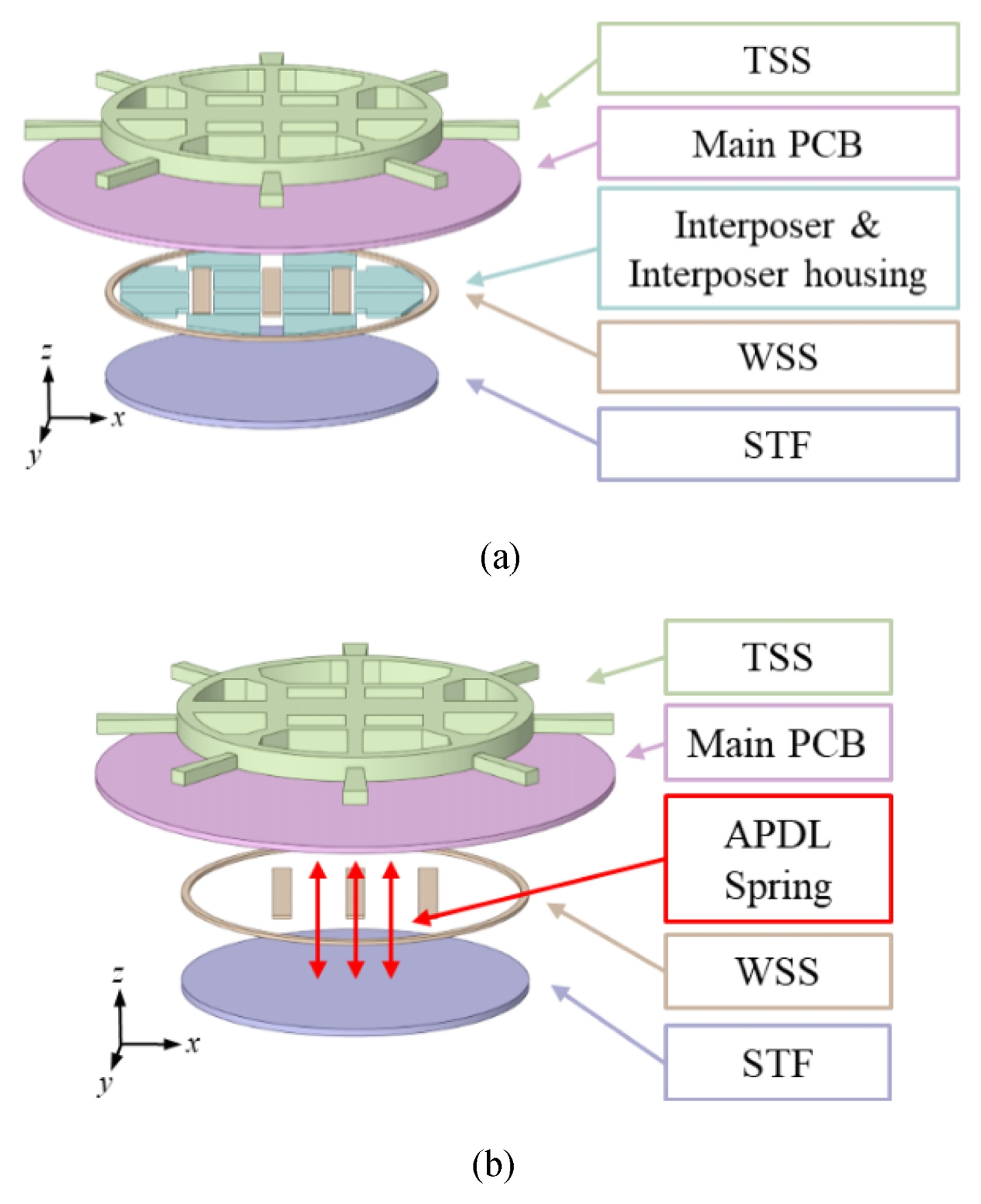
프로브 카드는 앞선 설명과 같이 TSS, Main PCB, 인터포저/하우징, STF, 그리고 프로브 팁으로 구성된다. 다만, 프로브 팁의 경우, 모델링의 크기가 상대적으로 매우 작으며, 그 수가 많아 본 해석에 포함시켰을 때 계산비용이 높아지는 문제가 발생하며, 또한 본 논문에서는 프로브 팁을 자세히 다루지 않기 때문에 프로브 팁을 제외한 TSS, Main PCB, 인터포저/하우징, 그리고 STF만을 모델링하였다.
본 논문에서 사용된 모델은 조건에 따라 3가지로 나뉘며,
Fig. 2에서 각 모델을 확인할 수 있다. Base Model은
Fig. 2(a)와 같이 인터포저/하우징을 포함한 TSS, Main PCB, 그리고 STF를 모두 모델링 하였으며 인터포저/하우징의 접촉조건은 Bonded의 강제 접촉을 입력하였다. 다음으로, Model 1은 인터포저/하우징을 제거하고 그 역할을 대체하기 위해 APDL 기반의 가상 스프링을 생성하여 적용했으며, 메시 생성은 Ansys Mechanical의 자동 메시(Auto Meshing)를 사용하였다. 마지막으로 Model 2는 Model 1과 동일하게 인터포저/하우징을 생략하고 APDL 가상 스프링을 적용하되, 자동 매시 대신 Point Cloud 기반 Meshing기법을 사용하였다.
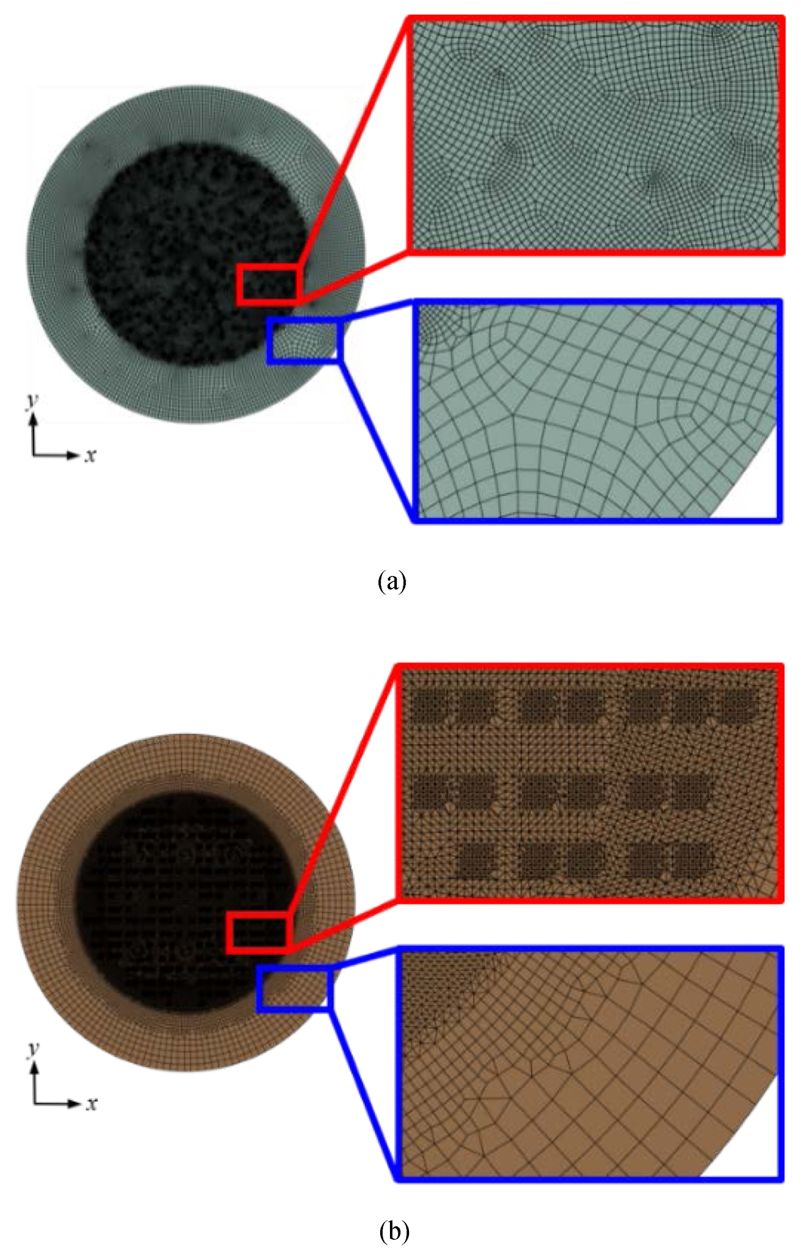
Point Cloud 기반 Meshing 기법은 CAD 모델의 메시에서 추출한 노드 좌표로 Point Cloud를 구성한 뒤 Python 코드를 사용해 목표 좌표에 정렬/재배치하고, 이를 활용하여 인터포저와 동일한 좌표에 메시를 생성 생성하는 방법으로,
Fig. 3에 Point Cloud Meshing기법을 활용해 생성된 Model 2의 노드 일부를 나타내었다.
Fig. 3에서 목표 좌표에 재배치된 노드를 확인할 수 있다.
Figs. 4(a)는 기존 자동 메시로 생성된 Model 1 - Main PCB의 메시를,
4(b)는 Point Cloud Meshing기법을 활용하여 생성된 Model 2 - Main PCB의 메시를 비교하여 보여주며, 4에서 볼 수 있듯 Point Cloud Meshing기법을 활용하여 스프링 생성부의 위치(X, Y, Z 좌표) 정확도를 높였음을 알 수 있다.
해석에 사용된 메시의 신뢰성은 주로 Mesh Quality와 Aspect Ratio로 평가된다. 선행 연구에 따르면 Trotta. A.등은 Element Quality가 최소 0.7 이상이면 해석에 활용하기에 신뢰할 수 있다고 보도했으며[
15], Jemaa. H.등은 모델의 Element 95%가 Aspect Ratio < 3을 만족할 때 고품질 메시로 간주하였다[
16].
본 논문에서 사용된 모델의 Element Quality는 Base Model과 Model 1에서 평균 0.92, Model 2에서 평균 0.79를 보였고, Aspect Ratio는 Base Model에서 1.48, Model 1에서 1.49, 그리고 Model 2에서 2.03의 평균값을 보였으며, 해당 내용은
Table 1에 정리하였다. 따라서 본 논문에 사용된 3가지 모델은 메시 품질 관점에서 신뢰성을 확보한 것으로 판단된다.
3.2.1 열해석 경계조건
Fig. 5(a)는 EDS 공정 중 웨이퍼 척에서 전달되는 열 조건을 반영하여 설정된 경계조건을 나타내었다. 프로브 카드 일부는 웨이퍼 검사 과정에서 진공환경에 놓이게 되는데, Main PCB의 하단 면을 포함한 그 하부(WSS, 인터포저/하우징, STF)는 WTS 장비 내부에서 진공환경에 놓이며, Main PCB 상부와 TSS는 상압의 실온 공기에 노출된다. 이에따라 상압환경의 상부 노출면에는 단순화된 대류 경계조건(Air, Simplified, 22°C)을 부여하였으며, 척으로부터 열을 직접 전달받는STF 전체에는 열을 모사하기 위해 100°C의 온도 조건을 적용하였다. 열해석의 결과는
Fig. 5(b)에서 확인할 수 있다. 해석 결과, 최대 100°C에서 최소 21.995°C까지의 온도 분포를 확인하였으며, 3가지 모델 모두 유사한 결과가 나타났다. 이후, 계산된 열의 데이터는 구조해석으로 전달되어 열-구조 연성 해석이 진행된다.
3.2.2 구조해석 경계조건
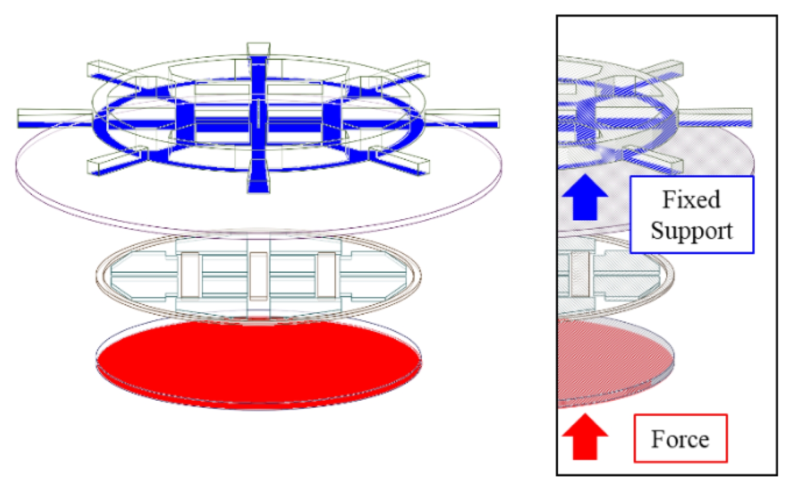
Fig. 6은 구조해석의 경계조건을 나타내었다. 최상단부의 TSS는 보강재로써 변형을 무시하여 TSS와 Main PCB의 접촉면(TSS 하부)에 Fixed Support를 입력하였다. STF의 하부 면에는 검사 중 프로브 핀이 웨이퍼에 접촉되며 가압될 때 발생하는 반력을 등가면하중으로 입력하였다.
접촉조건의 경우, Base Model에서 인터포저/하우징에 접촉하는 모든 접촉면에 실제와 같은 접촉조건을 입력하게 되면 해석이 수렴하지 않아, 실제 거동과 유사한 값을 얻을 수 있는 Bonded의 접촉조건으로 해석이 진행하였다. Model 1은 인터포저/하우징을 제거하고 APDL기반 가상 스프링으로 이를 대체하여 노드/접촉면의 수를 줄였다. 그러나 자동 메시로 생성된 노드의 좌표가 목 표 좌표와 일치하지 않아 스프링을 정확한 위치에 배치할 수 없었기에 추가과정이 필요하였는데, (i)
Fig. 7에 표시된 것처럼 스프링을 배치할 면(Face 1)과 마주 보는 면(Face 2)의 노드를 추출하고, (ii) Face 1, Face 2에서 추출한 노드 중, 목표 좌표와 최근접 대응 노드를 탐색한 뒤 쌍을 이루고, (iii) 매칭된 노드쌍 사이에 스프링 요소를 생성/연결하는 추가과정이 필요하였다. Model 2는 Model 1과 동일하게 인터포저/하우징을 APDL기반 가상 스프링으로 대체하였으며, 스프링 생성과정 중 목표 좌표에 노드를 생성하기 위해 Point Cloud Meshing기법을 추가로 용하였다.
4. 열-구조 연성 해석 결과
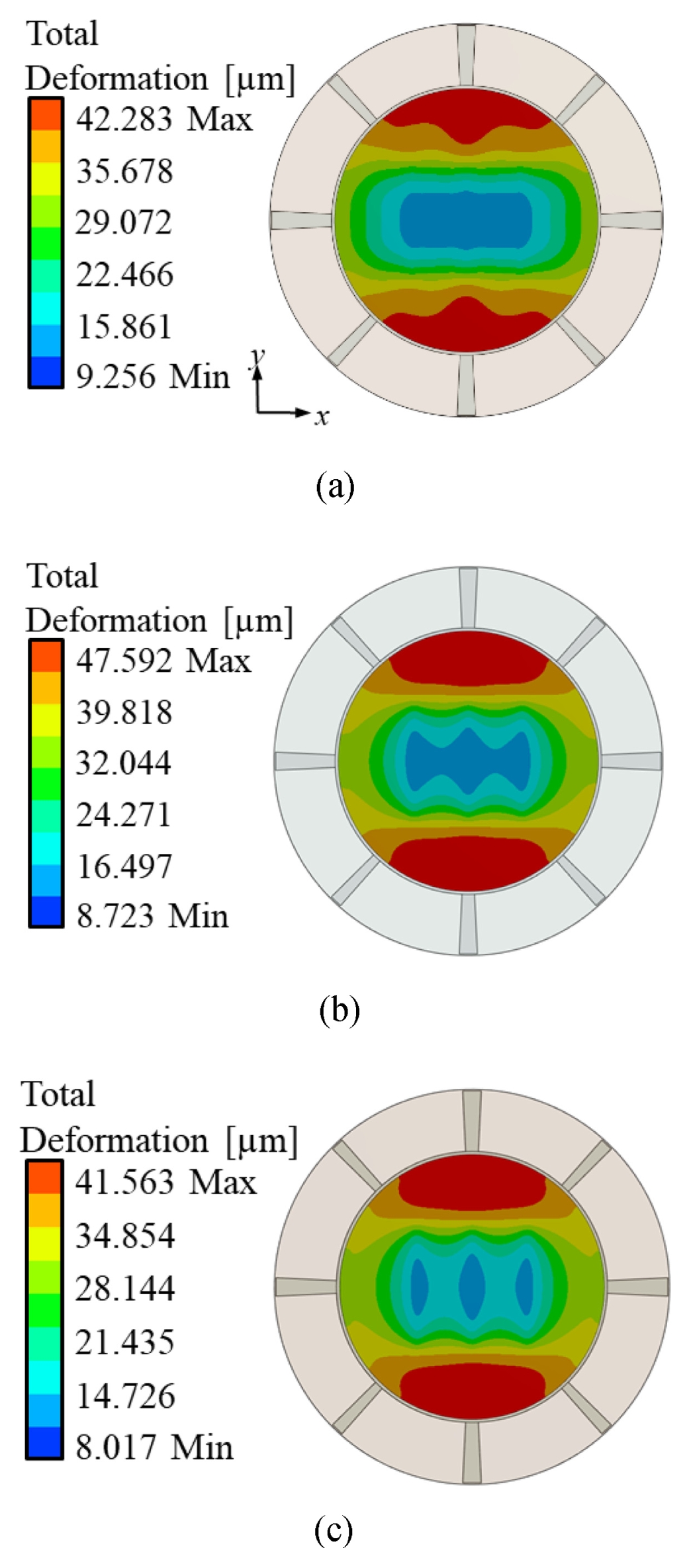
Figs. 8은 STF의 Total Deformation을 비교한 결과로,
8(a)는 Base Model로 최대 42.283 μm,
8(b)는 Model 1로 최대 47.592 μm,
Fig. 8(c)는 Model 2로, 최대 41.563 μm 변형을 보이며 세 모델은 모두 비슷한 최대변형량을 보였다. 해당 결과와 함께 각 모델들의 정보를
Table 2에 표로 정리하였다. Base Model은 인터포저/하우징을 포함한 전체를 모델링해서 노드와 접촉면 수가 33 개로 많은 접촉면을 보유하였으며, 그 결과 접촉조건에 의해 수렴성 저하의 문제가 발생했다. Model 1의 경우 앞서 언급한 과정을 통해 최근접 노드쌍을 확보하였으나, 자동 메시의 한계로 생성된 노드의 좌표가 목표 좌표와 정확히 일치하지 않아 해석 목표와 차이가 있을 것으로 보이는 반면, Model 2은 Model 1과 동일하게 인터포저/하우징의 모델링을 APDL 기반 가상 스프링으로 대체하되, 본 논문에서 제시한 Point Cloud Meshing기법을 활용하여 목표좌표에 정확히 노드를 위치시켰다. 그 결과, 스프링 연 결의 정확도를 확보할 수 있었으며, 실제 접촉 거동과 가장 유사한 결과를 얻을 수 있을 것으로 예상된다.
5. 결론
본 논문은 반도체 웨이퍼 검사용 프로브 카드의 열–구조 연성 해석에서 발생하는 접촉조건 문제를 해결하기 위해, APDL을 활용한 가상 스프링과 Point Cloud Meshing 방식을 사용한 해석방법을 제안하고 분석하였다. 비교 대상은 직접접촉 방식을 사용한 모델(Base Model), 자동 메시로 생성된 노드에 가상 스프링을 적용한 모델(Model 1), Point Cloud Meshing기법을 활용하여 원하는 좌표에 노드를 생성하여 가상의 스프링을 적용한 모델(Model 2) 이다. 그 결과는 다음과 같이 정리된다.
인터포저/하우징과 접촉한 다른 접촉면에 대한 해석에서 안정성을 확보할 수 있었다. Base Model에서 다수의 접촉면을 Bonded로 강제 접촉시키면서 발생한 실제 거동과의 차이는 Model 1, 2에서 인터포저/하우징의 모델링을 APDL기반의 가상 스프링으로 치환함으로써 해결하였다.
가상 스프링으로 접촉을 치환함으로써, 해석의 수렴성과 안정성을 확보하였다. 또한 Model 2는 Point Cloud Meshing기법을 활용하여 실제 거동과 가장 유사한 결과를 얻을 수 있을 것으로 예상된다.
해석 효율성이 증가하였다. APDL을 활용한 가상 스프링을 생성/적용한 모델(Model 1, 2)은 인터포저/하우징 모델링을 제거하여 노드/접촉면 수를 줄일 수 있었다. 특히 Model 2는 Point Cloud Meshing기법으로 필요 위치에만 노드를 생성함으로써 해석의 정확도를 높였으며, 해석 시간도 줄일 수 있었다.
본 논문에서 제안한 Point Cloud Meshing기법을 적용한 Model 2는 인터포저 수가 많은 대형/고밀도 프로브 카드에도 적용이 용이하며, 프로브 카드뿐만 아닌 다른 열–구조 연성 문제에서 접촉 대체 모델링에도 실용적인 대안이 될 수 있다.
본 논문에서는 유한요소 해석을 통해 프로브 카드의 열-구조 연성 해석에서 발생하는 접촉 문제 해결을 위한 새로운 방법을 제시하였다.
다만, 본 논문은 전산 모사를 중심으로 진행된 연구로, 해석 결과와 실제 실험치와 비교를 통한 검증이 필요하다. 향후 연구에서는 실험/검증을 통해 프로브 카드의 열-구조 연성 해석 신뢰성을 확보하고자 한다.
FOOTNOTES
-
ACKNOWLEDGEMENT
이 논문은 2025년도 정부(교육부)의 재원으로 한국산업기술진흥원조기취업형 계약학과 선도대학(원) 육성사업의 지원을 받아 수행된 연구임.
Fig. 1(a) Actual MEMS probe card, (b) Schematic diagram of WTS, and (c) Schematic diagram of probe card
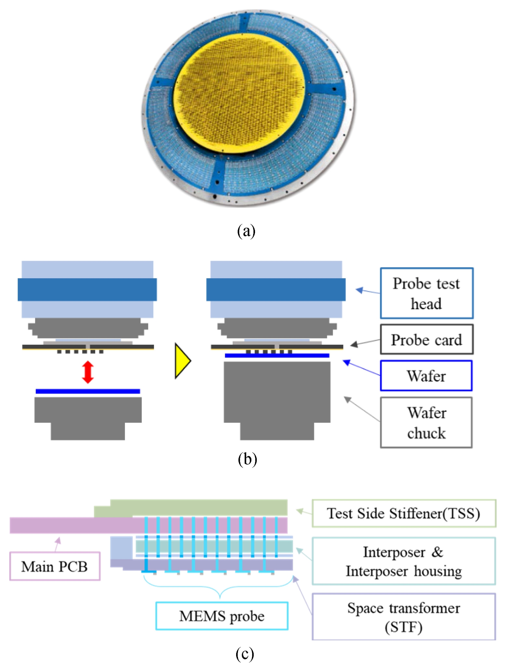
Fig. 2Finite element model of the probe card assembly. (a) Base model, with interposer & interposer housing, (b) Model 1&2, without interposer & interposer housing

Fig. 3Generated nodes using point cloud meshing
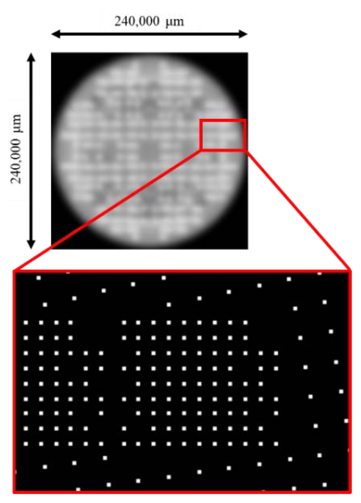
Fig. 4Mesh of Main PCB (a) Model 1: using auto meshing, (b) Model 2: using point cloud meshing

Fig. 5Temperature distribution from FE simulation. (a) Thermal conditions, and (b) Result of thermal analysis
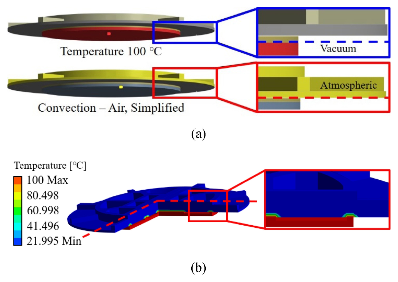
Fig. 6Boundary conditions for FE analysis of probe card

Fig. 7Spring connection Face 1, Face 2 pair for Model 1
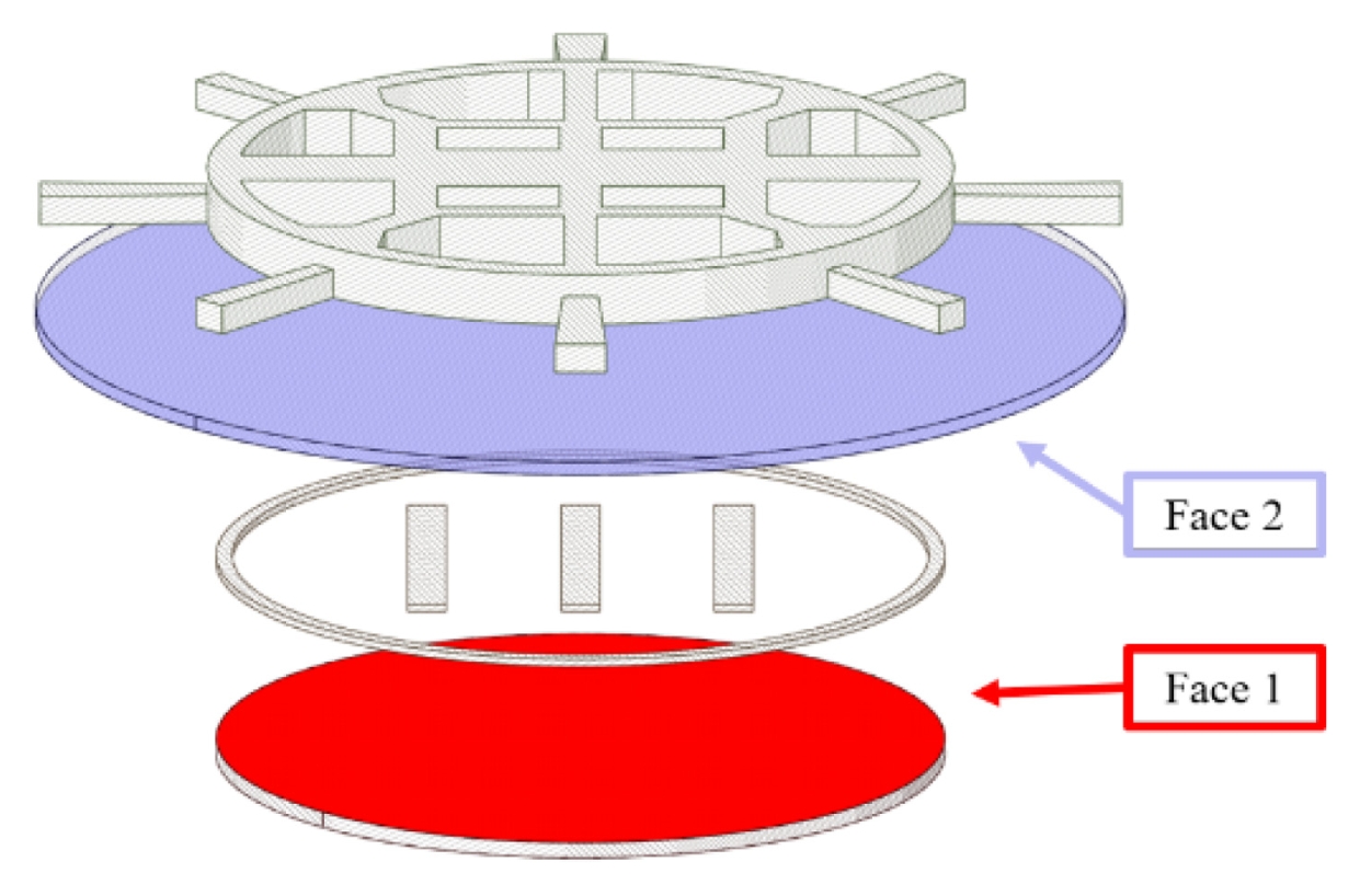
Fig. 8Comparison of total deformation among three models. (a) Base model, (b) Model 1, and (c) Model 2

Table 1Comparison of element quality and aspect ratio
Table 1
|
Base model |
Model 1 |
Model 2 |
|
Avg. element quality [−] |
0.92 |
0.92 |
0.79 |
|
Avg. aspect ratio [−] |
1.48 |
1.49 |
2.03 |
Table 2Summary of interpretation result by model
Table 2
|
Base model |
Model 1 |
Model 2 |
|
Number of node [−] |
865,871 |
802,859 |
669,235 |
|
Number of element [−] |
756,334 |
713,485 |
1,036,172 |
|
Number of contact surfaces [−] |
33 |
9 |
9 |
|
Maximum total deformation [μm] |
42.28 |
47.59 |
41.56 |
|
CP time [sec] |
5485.25 |
1818.91 |
837.03 |
REFERENCES
- 1. Sun, L., Bai, C., Sarkis, J., (2024), Environmental and social performance relationships to firm efficiency: Evidence from the semiconductor industry, International Journal of Production Economics, 278, 109410.
- 2. Foscale, T., Bernardi, P., (2025), A cost–benefit analysis of multi-site wafer testing, Electronics, 14(12), 2450.
- 3. Yoon, H. J., Chae, J., (2019), Simulation study for semiconductor manufacturing system: Dispatching policies for a wafer test facility, Sustainability, 11(4), 1119.
- 4. Kim, M., Hong, W. S., Kim, M.-S., (2022), Laser soldering process optimization of mems probe of probe card for semiconductor wafer test, Journal of Welding and Joining, 40(3), 271-277.
- 5. Kang, S., Nah, W., (2023), Research on design technology to minimize signal distortion of probe card with many branches, Journal of the Institute of Electronics and Information Engineers, 60(9), 13-23.
- 6. Chang, Y.-H., Yin, J.-J., Suh, Y.-S., (2010), Optimization of thermal deformation in probe card, Journal of the Korea Academia-Industrial Cooperation Society, 11(11), 4121-4128.
- 7. Park, J., (2021), Study on the improvement of thermal deformation in probe card, M.Sc. Thesis, Seoul National University of Science and Technology.
- 8. Kwon, H.-J., Lee, J., Shin, B., Jeon, S., Han, C. S., Im, C. M., (2014), Geometry design of vertical probe needle using mechanical testing and finite element analysis, International Journal of Precision Engineering and Manufacturing, 15(11), 2335-2342.
- 9. Hyun, D.-E., Jeon, J.-B., Lee, Y.-S., Kim, Y-N, Kim, M, Ko, S., Koo, S.-M., Shin, W. H., Park, C., Lee, D.-W., (2022), Fabrication of large-area mullite–cordierite composite substrates for semiconductor probe cards and enhancement of their reliability, Materials, 15(12), 4283.
- 10. Wong, J. C., Soon, K. H., Kim, H. C., Kho, D. C. T., Chan, C. Y. W., (2023), Modeling of the impact of mechanical stress resulted from wafer probing and wire bonding on circuit under pad, Microelectronics Reliability, 151, 115240.
- 11. Le, X. L., Choa, S.-H., (2021), Design of new au–nico mems vertical probe for fine-pitch wafer-level probing, Crystals, 11(5), 485.
- 12. Ansys Inc, APDL: The language of simulation. https://www.ansys.com//blog/what-is-apdl
- 13. Yoo, D.-J., (2006), Automatic nurbs surface generation from unorganized point cloud data, Journal of the Korean Society for Precision Engineering, 23(9), 200-207.
- 14. Castellazzi, G., Presti, N. L., D’Altri, A. M., De Miranda, S., (2022), Cloud2fem: A finite element mesh generator based on point clouds of existing/historical structures, SoftwareX, 18, 101099.
- 15. Trotta, A., Clark, J. M., McGoldrick, A., Gilchrist, M. D., Annaidh, A. N., (2020), Biofidelic finite element modelling of brain trauma: Importance of the scalp in simulating head impact, International Journal of Mechanical Sciences, 173, 105448.
- 16. Jemaa, H., Eisenburger, M., Greuling, A., (2024), Semi-automated generation of bone loss defects around dental implants and its application in finite element analysis, Computer Methods in Biomechanics and Biomedical Engineering, 27(13), 1756-1767.
Biography
- Seong Hoon Kim
M. S. candidate in the Depart of Smart Mobility Engineering, Kongju National University. His research interest is FEA.
- Min Seong Oh
Ph. D. candidate in the Department of Future Convergence Engineering, Kongju National University. His research interest is FEA.
- Ji Eun Kim
Sr. Manager of TSE Group Strategy Planning_ Technology Strategy.
- Kyeong Hoon Lee
Staff Engineer of TSE Group Strategy Planning_ Technology Strategy.
- Seok Moo Hong
Professor in the Department of Future Automotive Engineering, Kongju National University. His research interest is Metal Sheet Forming and Forging, FEA, Optimizing.